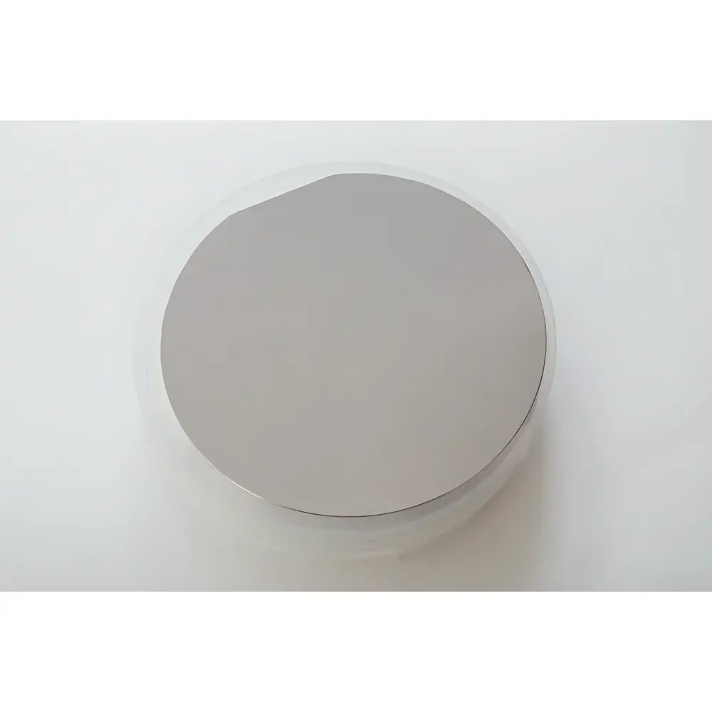
Silicon Wafer with Nickel (111)-Oriented Thin Film Coating
| Brand | 合肥科晶 |
|---|---|
| Origin | USA |
| Manufacturer Type | General Distributor |
| Origin Category | Imported |
| Model | Si镀Ni薄膜 |
| Price | Upon Request |
| Silicon Substrate | P-type, B-doped, <100±0.5° orientation, Ø4" ±0.5 mm × 0.525 ±0.025 mm, single-side polished, resistivity 1–20 Ω·cm |
| Ni Film Thickness | 100 nm |
| Ni Crystallographic Orientation | <111>-oriented polycrystalline |
| Packaging | Vacuum-sealed in Class 100 cleanroom bags within Class 1000 cleanroom environment, or individual wafer cassette |
Overview
This product is a high-purity silicon (Si) wafer substrate coated with a precisely controlled 100 nm nickel (Ni) thin film exhibiting strong crystallographic texture. Engineered for advanced materials research and thin-film device fabrication, the wafer serves as a functional platform for studies in spintronics, magnetic heterostructures, seed layers for electroplating, and interfacial physics under ultrahigh vacuum (UHV) or controlled ambient conditions. The underlying Si substrate is a standard 4-inch diameter, single-side polished wafer with tightly specified crystallographic orientation (<100±0.5°), thickness tolerance (0.525 ±0.025 mm), and electrical resistivity (1–20 Ω·cm), ensuring compatibility with semiconductor-grade processing tools including sputtering systems, MBE chambers, and ex-situ characterization platforms such as XRD, XPS, and MOKE.
Key Features
- P-type boron-doped silicon substrate meeting SEMI-standard dimensional and crystalline specifications for 4-inch wafers
- Uniform 100 nm nickel thin film deposited via physical vapor deposition (PVD) under controlled conditions to achieve dominant preferred orientation
- High degree of polycrystalline coherence confirmed by X-ray diffraction (XRD) θ–2θ scans and pole figure analysis
- Single-side polished surface finish optimized for epitaxial or textured growth initiation
- Class 1000 cleanroom handling and Class 100 cleanroom vacuum packaging to minimize particulate contamination and native oxide formation
- Available in both full 4-inch wafer format and cut 10×10 mm square chips for rapid prototyping and small-area measurements
Sample Compatibility & Compliance
The wafer is compatible with standard photolithography, lift-off, ion milling, and thermal annealing processes up to 400 °C in inert or reducing atmospheres. Its -textured Ni layer provides enhanced magnetic anisotropy and improved lattice matching for subsequent deposition of ferromagnetic or antiferromagnetic overlayers (e.g., CoFeB, IrMn). While not certified to ISO 9001 or ASTM F1529 per se—given its status as a research-grade consumable—the manufacturing and packaging protocols adhere to industry-recognized cleanroom practices aligned with SEMI C1–C23 standards for silicon wafer handling. Documentation includes substrate certification of conformance (CoC) detailing orientation, doping type, resistivity range, and thickness verification.
Software & Data Management
As a passive substrate material, this Si/Ni wafer does not incorporate embedded electronics or firmware. However, it is fully compatible with industry-standard metrology software suites used in thin-film characterization workflows—including Bruker DIFFRAC.EVA for XRD phase identification, Thermo Avantage for XPS peak deconvolution, and JADE for texture analysis. Raw diffraction data, AFM topography files (.wsx, .spm), and sheet resistance maps generated from four-point probe measurements can be exported in ASCII or CSV formats for integration into LIMS or ELN systems compliant with 21 CFR Part 11 requirements when paired with validated laboratory instruments.
Applications
- Model system for studying perpendicular magnetic anisotropy (PMA) in Ni-based multilayers
- Seed layer for electrodeposition of Ni–Fe or Ni–Co alloys in microelectromechanical systems (MEMS)
- Substrate for in-situ synchrotron-based surface diffraction and reflectivity experiments
- Benchmark reference for calibrating magnetron sputtering chamber parameters (power, pressure, bias)
- Platform for investigating interfacial diffusion kinetics between Ni and transition metal oxides (e.g., Ni/SrTiO₃)
- Test vehicle for developing low-temperature bonding techniques in heterogeneous integration
FAQ
Is the Ni film amorphous or crystalline?
The Ni film is polycrystalline with strong preferred orientation, as verified by XRD pole figure analysis.
Can the wafer be cleaned using standard RCA protocols?
Yes—standard SC1 (NH₄OH:H₂O₂:H₂O) and SC2 (HCl:H₂O₂:H₂O) treatments are compatible; however, prolonged exposure to SC1 may slightly oxidize the Ni surface. A final dilute HCl dip is recommended prior to UHV loading.
What is the typical root-mean-square (RMS) roughness of the Ni surface?
Surface roughness is not routinely measured or guaranteed for this batch-manufactured research substrate; users requiring quantitative AFM metrics should perform in-house characterization or request custom metrology add-ons.
Are custom thicknesses or alternative orientations available?
Yes—custom Ni thicknesses (50–500 nm) and alternate orientations (e.g., ) can be produced upon request with extended lead time and minimum order quantities.
Does the product include traceability documentation?
Each shipment includes a Certificate of Conformance listing batch number, substrate origin, coating date, and key metrological attributes recorded during final QA inspection.