Si+SiO2+Si3N4 Tri-Layer Thin-Film Substrate (Imported Grade) –合肥科晶 Model Si/SiO₂/Si₃N₄
| Brand | Hefei Kejing |
|---|---|
| Origin | USA |
| Manufacturer Type | Authorized Distributor |
| Origin Category | Imported |
| Model | Si/SiO₂/Si₃N₄ Tri-Layer Thin-Film Substrate |
| Pricing | Available Upon Request |
Overview
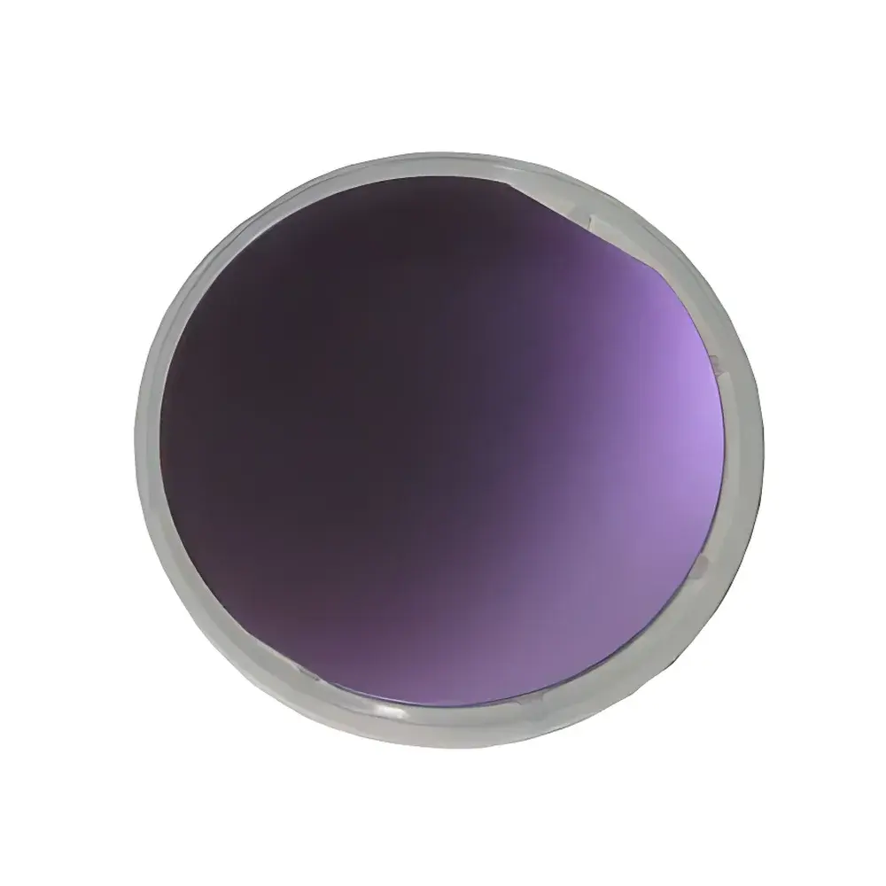
The Si/SiO₂/Si₃N₄ Tri-Layer Thin-Film Substrate (Imported Grade) is a precision-engineered silicon-based platform designed for advanced microfabrication, MEMS development, photonic device prototyping, and high-fidelity thin-film process validation. This substrate integrates three functionally distinct layers—single-crystal silicon (Si), thermally grown silicon dioxide (SiO₂), and low-stress silicon nitride (Si₃N₄)—in a monolithic, wafer-level architecture. The stack is fabricated using industrial-grade thermal oxidation (dry O₂ at 1000 °C) and low-pressure chemical vapor deposition (LPCVD), ensuring atomic-level interface integrity, minimal interfacial defect density, and high reproducibility across production lots. Its primary measurement principle relies on the controlled optical and electrical contrast between layers, enabling precise ellipsometric thickness calibration, stress mapping via wafer curvature analysis, and dielectric characterization under standardized test conditions (ASTM F39–22, ISO 14644-1 Class 1000 cleanroom handling).
Key Features
- Monolithic tri-layer architecture: -oriented p-type boron-doped Si wafer (resistivity 0.01–0.1 Ω·cm), thermally grown SiO₂ (300 nm ±5 nm), and LPCVD-deposited Si₃N₄ (50 nm ±3 nm), both layers deposited on both sides
- High geometric fidelity: Diameter 50.8 mm ±0.5 mm, thickness 250 µm ±25 µm, with double-side chemical-mechanical polishing (CMP) achieving surface roughness <0.3 nm RMS
- Optical uniformity: Refractive index of SiO₂ layer confirmed at 1.455 ±0.002 @ 633 nm (ellipsometry traceable to NIST SRM 2033)
- Process-ready packaging: Supplied in ISO Class 5 (100-particle/ft³) cleanroom bags under vacuum or individual SEMI-standard cassette-compatible single-wafer carriers
- Functional yield: ≥80% usable area defined by absence of particles >0.5 µm, edge chipping, or delamination per SEM/EDS inspection
Sample Compatibility & Compliance
This substrate is fully compatible with standard semiconductor processing tools including plasma etchers (ICP/RIE), sputter coaters, e-beam evaporators, and rapid thermal processors (RTP). It meets material requirements for ASTM F1570 (Silicon Wafer Specifications), SEMI MF1530 (Thickness Uniformity), and ISO 10110-7 (Surface Quality for Optical Components). All wafers undergo full-lot metrology verification—including spectral reflectance, four-point probe sheet resistance, and interferometric thickness mapping—prior to release. Documentation includes CoA (Certificate of Analysis) with lot-specific data, supporting GLP-compliant R&D workflows and FDA 21 CFR Part 11–aligned quality records when integrated into validated lab information management systems (LIMS).
Software & Data Management
While the substrate itself is a passive physical reference standard, its metrological traceability supports integration with industry-standard analytical platforms: SpectraRay™ (Sentech), FilmTek™ (SCI), and Woollam VASE ellipsometers for non-contact thickness and n/k modeling; KLA-Tencor Surfscan SP5 or Hitachi CG4000 for defect quantification; and Bruker DektakXT or Veeco NT9100 for step-height profiling. Raw measurement datasets can be exported in ASTM E1395-compliant .csv or .xml formats. Audit trails, instrument calibration logs, and operator metadata are retained in accordance with ISO/IEC 17025:2017 clause 7.7 (Results Reporting) when used within accredited laboratories.
Applications
- Calibration reference for optical thin-film metrology systems (ellipsometry, reflectometry, interferometry)
- Baseline substrate for evaluating etch selectivity, deposition uniformity, and stress-induced bow in SiN/SiO₂ multilayer stacks
- Platform for developing CMOS-compatible MEMS resonators, microcantilevers, and optomechanical sensors
- Test vehicle for low-k dielectric integration studies and interfacial trap density (Dit) extraction via capacitance-voltage (C-V) and conductance-frequency (G-f) methods
- Research-grade support for quantum photonics waveguide fabrication, where Si₃N₄ layer serves as low-loss guiding medium atop SiO₂ cladding
FAQ
Can custom thicknesses be ordered beyond the standard 300 nm SiO₂ / 50 nm Si₃N₄ stack?
Yes. Thickness customization from 50 nm to 1000 nm per layer is available upon technical review and minimum order quantity agreement.
Is the Si substrate double-side polished and what surface finish is guaranteed?
Yes—both sides are CMP-polished to ≤0.3 nm RMS roughness, verified per ISO 10110-7 specifications.
Are lot-specific metrology reports provided with each shipment?
Yes. Each order includes a Certificate of Analysis containing ellipsometric thickness maps, refractive index values, resistivity measurements, and particle count data.
Does this substrate comply with RoHS and REACH regulations?
Yes. All constituent materials and processing chemicals are certified RoHS Directive 2011/65/EU and REACH Annex XVII compliant.
What is the recommended storage condition to maintain film integrity?
Store in original vacuum-sealed Class 100 bag at ambient temperature (15–25 °C), away from UV exposure and humidity >40% RH.

 System")