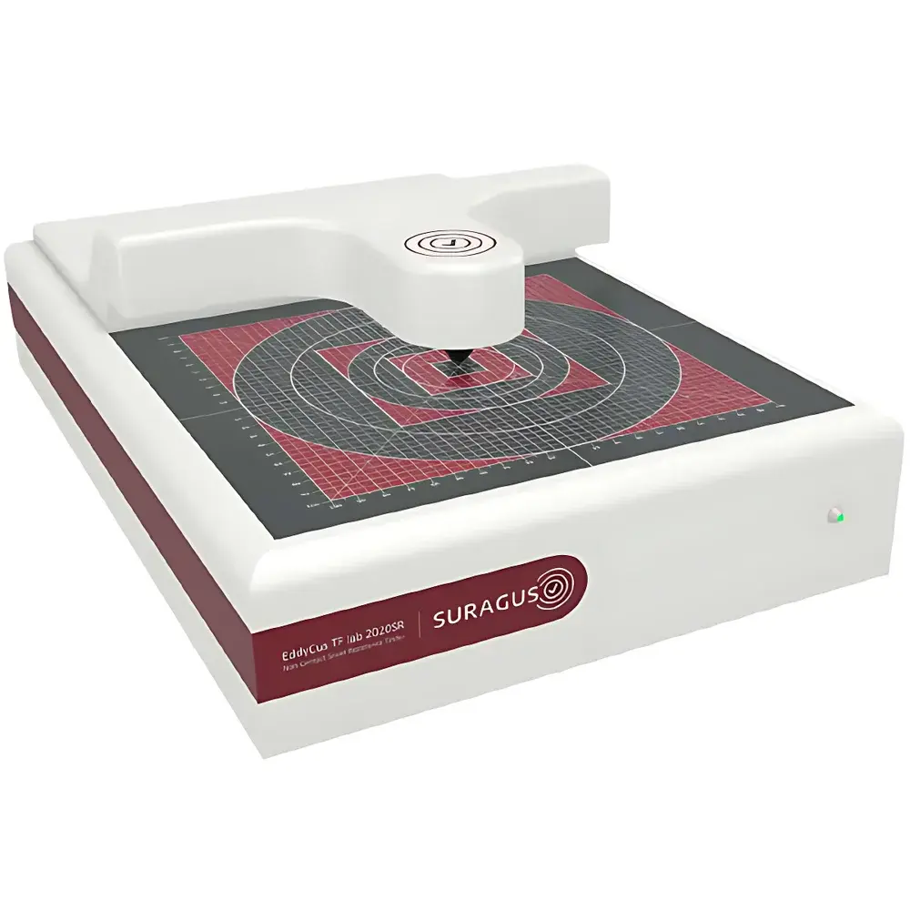
SURAGUS EddyCus TF lab 2020 Non-Contact Sheet Resistance and Thin-Film Thickness Analyzer
| Brand | SURAGUS |
|---|---|
| Origin | Germany |
| Model | TF lab 2020 |
| Measurement Principle | Eddy Current |
| Sheet Resistance Range | 0.0001–100,000 Ω/□ (3 accuracy tiers) |
| Thickness Range (e.g., Cu) | 2 nm – 2 mm |
| Max Sample Size | 204 × 204 mm (8″ square) |
| Sensor Gap Options | 1 / 2 / 5 / 10 / 25 mm |
| Accuracy | 1–8% depending on range |
| Dimensions (W×D×H) | 290 × 445 × 140 mm |
| Weight | 10 kg |
| Compliance | CE, RoHS, ISO/IEC 17025-compatible operation |
Overview
The SURAGUS EddyCus TF lab 2020 is a precision-engineered, non-contact eddy current-based analyzer designed for laboratory-scale characterization of conductive thin films. It simultaneously quantifies sheet resistance (Rs, in Ω/□) and metallic film thickness (in nm or µm) without physical contact, eliminating risk of surface damage, probe wear, or measurement-induced heating. The instrument operates on the principle of electromagnetic induction: a high-frequency alternating magnetic field generated by a miniature coil induces eddy currents in the conductive layer; the resulting perturbation in coil impedance is calibrated against known standards to derive Rs and—via established conductivity–thickness relationships—film thickness. This physics-based methodology ensures traceable, reproducible results across diverse substrates including glass, silicon wafers, polymer foils, and ceramic carriers. Its open-frame design accommodates samples up to 204 × 204 mm with three unobstructed edges, enabling rapid manual positioning and compatibility with large-area architectural glass, display panels, and photovoltaic substrates.
Key Features
- True non-contact measurement using calibrated eddy current sensing—no electrode alignment, pressure loading, or surface preparation required
- Multi-range sheet resistance capability: 0.0001–10 Ω/□ (low-range), 0.01–1,000 Ω/□ (standard), and 10–100,000 Ω/□ (high-range), each with defined accuracy envelopes (1–8%)
- Simultaneous derivation of metal film thickness (e.g., Cu, Al, Ag, NiCr) from 2 nm to 2 mm, validated against reference standards per ISO 14644-1 cleanroom-grade calibration protocols
- Modular sensor gap configuration (1 / 2 / 5 / 10 / 25 mm) to accommodate varying substrate warpage, encapsulation layers, or protective coatings
- Integrated motorized Z-axis fine adjustment for repeatable sensor-to-sample distance control within ±1 µm resolution
- Rugged aluminum chassis (290 × 445 × 140 mm, 10 kg) with vibration-damped feet and EMI-shielded electronics for stable operation in shared lab environments
Sample Compatibility & Compliance
The TF lab 2020 supports a broad spectrum of conductive and semi-conductive thin-film systems on rigid or semi-rigid substrates. Validated material classes include sputtered or evaporated metal films (Ag, Cu, Al, ITO, AZO), printed conductive inks (Ag nanoparticle, PEDOT:PSS), CVD-grown graphene and carbon nanotube networks, electroplated metallization layers, and transparent conductive oxides used in touch sensors and smart windows. Substrate compatibility extends to soda-lime glass, borosilicate, fused silica, Si/SiO₂ wafers, PET/PEN foils, and anodized aluminum. The system meets CE marking requirements and complies with RoHS Directive 2011/65/EU. While not a certified metrology standard, its measurement workflow aligns with ISO/IEC 17025:2017 clause 7.2 (method validation) and supports GLP documentation through audit-trail-enabled software logging. For regulated environments (e.g., semiconductor fab QC or medical device coating verification), optional IQ/OQ documentation packages are available upon request.
Software & Data Management
Operation is guided by SURAGUS’ proprietary EddyCus Control Suite v4.x—a Windows-based application supporting both manual point measurement and automated grid mapping (up to 100 × 100 points). The interface provides real-time Rs and thickness overlays, statistical summary (mean, σ, min/max, CV%), and export in CSV, XML, or industry-standard .tdms format. All measurements embed metadata: timestamp, operator ID, sensor gap setting, calibration ID, and environmental conditions (optional external temperature/humidity input). Audit trails record every parameter change, data export, and calibration event—enabling compliance with FDA 21 CFR Part 11 when paired with network-authenticated user accounts and digital signature modules. Raw impedance spectra and calibration coefficients are stored in encrypted binary archives for retrospective reprocessing.
Applications
- Quality assurance of low-emissivity (Low-E) architectural glass coatings during inline production and incoming inspection
- R&D validation of transparent electrodes for OLED lighting, micro-LED backplanes, and capacitive touch sensors
- Thickness uniformity assessment of electroplated copper layers in PCB and advanced packaging substrates
- Process development monitoring for roll-to-roll printed electronics, including silver nanowire and graphene oxide films
- Failure analysis of delamination or oxidation in multilayer conductive stacks (e.g., Ti/Ag/Ti on PET)
- Non-destructive verification of anti-static coatings on pharmaceutical blister packaging and cleanroom garments
FAQ
Does the TF lab 2020 require electrical contact with the sample?
No. It uses non-contact eddy current induction and does not require probe placement, grounding, or sample biasing.
Can it measure non-metallic conductive films like ITO or PEDOT:PSS?
Yes—provided the material exhibits sufficient bulk conductivity (σ > ~10 S/m); measurement accuracy is optimized for films with carrier mobility ≥1 cm²/V·s.
Is calibration traceable to national standards?
Calibration is performed using NIST-traceable thin-film resistance standards (e.g., PTB-certified Cr/NiCr reference wafers) and verified annually per internal SOP-EDDY-003.
What substrate flatness tolerance is acceptable?
For 1 mm sensor gap, maximum allowable deviation is ±25 µm over 10 mm; for 25 mm gap, tolerance increases to ±200 µm.
Can the system integrate into an automated production line?
The TF lab 2020 is a benchtop R&D instrument; for inline integration, SURAGUS offers the industrial-grade EddyCus TF inline series with PLC interface and Ethernet/IP support.


