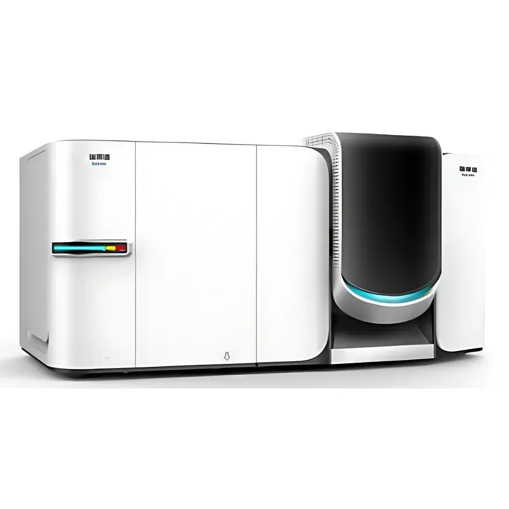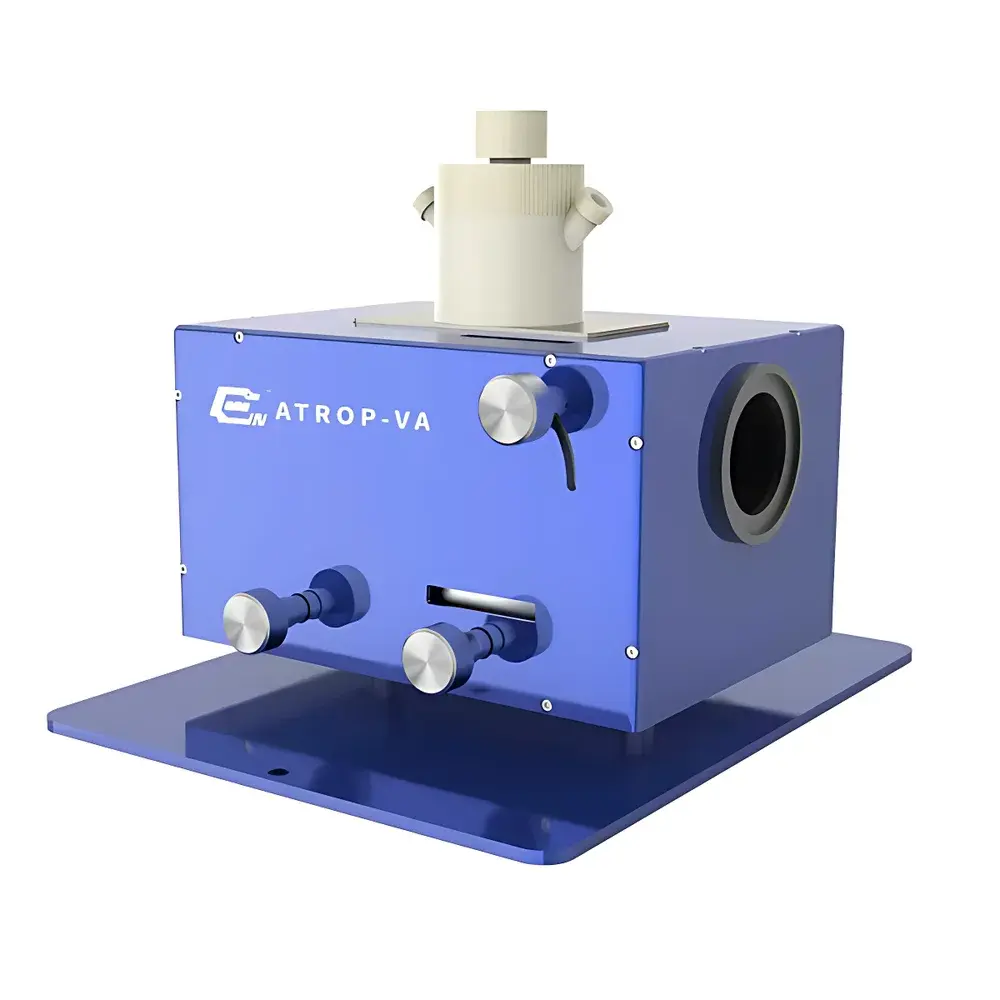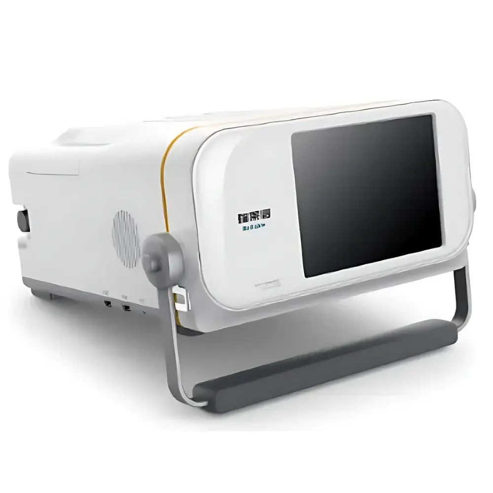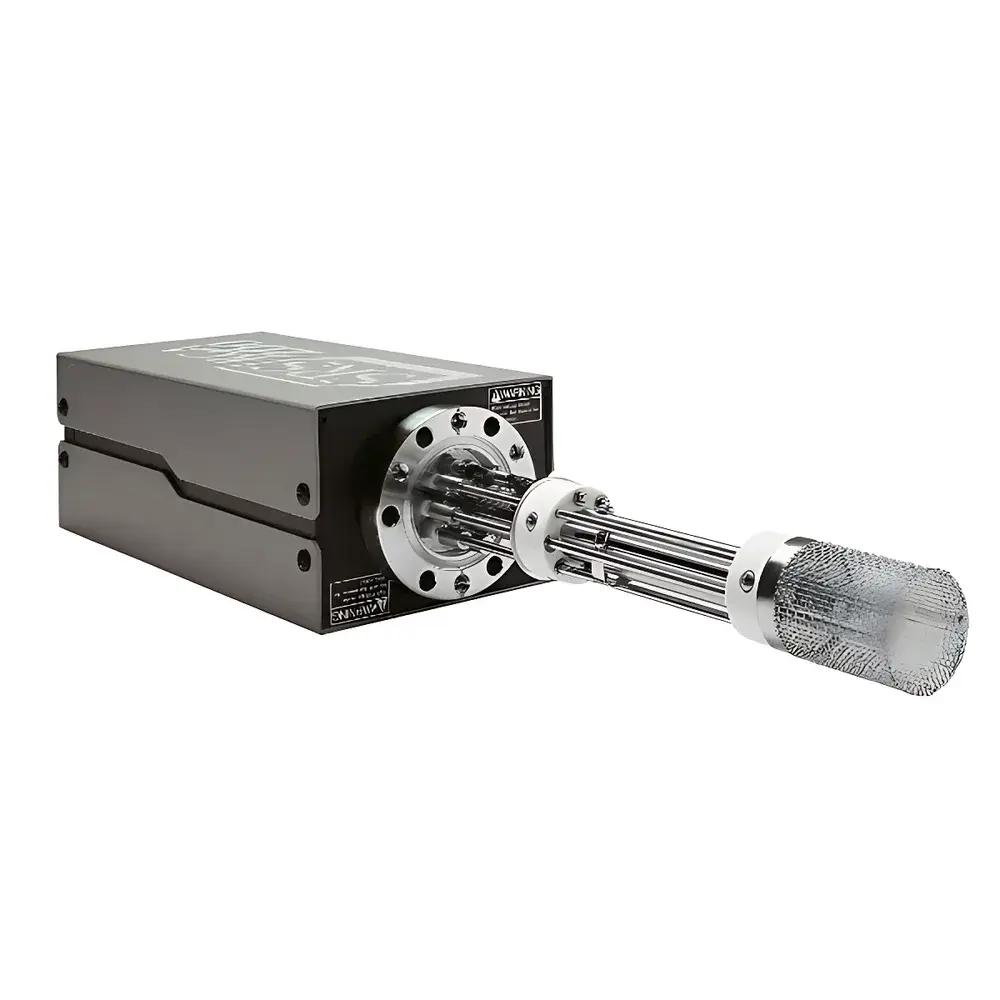
Suragus EddyCus TF Series Non-Contact Thin-Film Sheet Resistance Meters
| Brand | Suragus (distributed by Auniontech) |
|---|---|
| Origin | Shanghai, China |
| Manufacturer Type | Authorized Distributor |
| Instrument Category | Electrochemical Instrument Accessory |
| Measurement Principle | Non-contact eddy current sensing |
| Substrate Compatibility | Glass, silicon wafers, polymer foils, OLED/LED substrates, Low-E coated glass, graphene layers, conductive textiles, PV cells |
| Max. Sample Size (Lab) | 204 mm × 204 mm (8″) |
| Max. Scanning Area (Map) | 300 mm × 300 mm (12″) |
| Sensor Gap Options | 3 / 5 / 10 / 15 / 25 mm |
| Sheet Resistance Range | 10⁻⁴ – 2×10⁵ Ω/sq (6 decades, VLSR to VHSR) |
| Thickness Measurement (e.g., Cu) | 2 nm – 2 mm |
| Repeatability (2σ) | < 0.3%–1% depending on range |
| Accuracy | ±1% to ±5% (range-dependent) |
| Software | SURAGUS Control & Analysis Suite (with SDK support) |
| Compliance | Designed for GLP-compliant lab environments |
Overview
The Suragus EddyCus TF Series comprises a family of non-contact, eddy current–based instruments engineered for precise, repeatable sheet resistance (Rs) characterization of conductive thin films and metallized layers—without physical contact, surface preparation, or electrical probing. Unlike conventional four-point probe (4PP) or van der Pauw methods, which require ohmic contact, lithographic test structures, and are highly sensitive to surface topography or passivation layers, the EddyCus TF platform operates on electromagnetic induction: an alternating magnetic field from a high-frequency coil induces eddy currents in the conductive layer; the resulting perturbation in the coil’s impedance is quantitatively correlated to Rs via calibrated inverse modeling. This principle enables reliable measurement through dielectric encapsulants (e.g., SiO₂, SiNx, polymer overcoats), across curved or fragile substrates (e.g., automotive windshields, flexible OLEDs), and on buried interconnects inaccessible to contact probes. The system is inherently insensitive to surface roughness, oxidation, or ambient humidity—critical for in-line QC of transparent conductive oxides (TCOs), sputtered ITO/Ag grids, evaporated metal electrodes, and emerging 2D materials such as graphene and MXenes.
Key Features
- True non-contact operation: No mechanical wear, zero risk of film damage or contamination—ideal for delicate or production-integrated samples.
- Multi-range sensor architecture: Single-sensor coverage across six decades of sheet resistance (100 µΩ/sq to 200 kΩ/sq), segmented into VLSR, LSR, MSR, HSR, and VHSR modes for optimized signal-to-noise ratio and accuracy per regime.
- Real-time, single-point measurement (TF Lab 2020SR): Sub-second acquisition at fixed lift-off distance; intuitive touchscreen interface with live Rs and estimated metal thickness display.
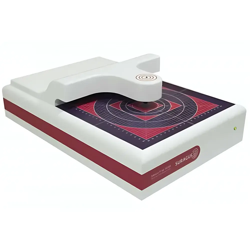
- High-resolution spatial mapping (TF Map 2530SR): Motorized XY stage enables programmable scanning up to 300 × 300 points (90,000 data points) over 300 mm × 300 mm areas; edge-effect correction algorithms (2–10 mm exclusion zone) ensure metrologically valid boundary data.
- Portable handheld variant (TF Portable 1010SR): Battery-powered (Li-ion, >20 h runtime), compact form factor (87 × 178 × 48 mm), and Bluetooth-enabled—designed for factory-floor QA, incoming inspection, and field service of architectural glass, touch panels, and battery electrode coatings.
- Robust calibration traceability: Factory-calibrated against NIST-traceable standards; optional annual recalibration service available with full uncertainty budget documentation.
Sample Compatibility & Compliance
The EddyCus TF Series accommodates diverse substrate geometries and material systems—including rigid (silicon wafers, borosilicate glass), semi-rigid (PET/PEN foils), and conformal (curved automotive glazing)—without fixture adaptation. It measures through non-conductive layers up to 100 µm thick (e.g., anti-reflective stacks, moisture barriers), provided the underlying conductor exhibits sufficient conductivity contrast. The instrument complies with fundamental metrological requirements for laboratory use under ISO/IEC 17025:2017 frameworks. While not a regulated medical device, its data export capabilities (CSV/TXT/XML with timestamps, operator ID, and measurement parameters) support FDA 21 CFR Part 11–aligned electronic record practices when integrated into validated QA workflows. All firmware and software enforce user-level access control, audit trails for parameter changes, and immutable raw-data logging—facilitating GLP/GMP-aligned documentation for semiconductor, photovoltaic, and display manufacturing.
Software & Data Management
Control and analysis are performed via the SURAGUS Control & Analysis Suite—a Windows-based application featuring a modular, touch-optimized GUI. Core functions include real-time Rs and thickness visualization, manual point-and-measure navigation, automated grid mapping with customizable pitch (1–25 mm), statistical reporting (mean, std dev, min/max, histogram), and defect-highlighting overlays. Raw data files embed full metadata: sensor ID, calibration date, lift-off distance, excitation frequency, temperature, and environmental conditions. The SURAGUS Software Development Kit (SDK) provides C++ and Python APIs for integration into custom MES, SPC, or automation platforms (e.g., LabVIEW, MATLAB, Python-based analytics pipelines). Export formats include comma-separated values (CSV) for Excel/SPC tools, XML for LIMS ingestion, and proprietary .sur files for reprocessing with updated calibration models.
Applications
- Quality assurance of low-emissivity (Low-E) architectural glass coatings during float-glass production.
- In-process monitoring of ITO, AZO, or Ag-nanowire layers on flexible OLED backplanes and touch sensors.
- Uniformity mapping of metal seed layers (Cu, Al, TiW) on 200 mm and 300 mm semiconductor wafers pre- and post-CMP.
- R&D validation of graphene CVD transfer quality, including domain continuity and doping homogeneity.
- Electrode sheet resistance profiling in lithium-ion battery dry electrode coating lines (anode/cathode foils).
- Conductivity screening of printed electronics (Ag nanoparticle inks, PEDOT:PSS) on paper or textile substrates.
FAQ
Can the EddyCus TF measure through thick insulating layers?
Yes—measurement is possible through dielectric overlayers up to ~100 µm thick (e.g., SiO₂, photoresist, acrylic), provided the conductive layer beneath has sufficient conductivity and lateral continuity. Signal attenuation increases with insulator thickness and permittivity; optimal performance is achieved with ≤25 µm encapsulation.
Does surface roughness affect measurement accuracy?
No—eddy current coupling depends on bulk conductivity and geometry, not surface morphology. Unlike optical reflectance or contact resistance methods, Rs values remain stable across RMS roughness values up to several hundred nanometers.
Is calibration required before each measurement?
No—factory calibration is stable over time and temperature (±0.01%/°C drift compensated in firmware). Users perform a one-time reference measurement on a certified standard wafer or foil upon system installation; subsequent measurements require no recalibration unless sensor hardware is replaced.
Can the system quantify anisotropic conductivity?
Yes—the TF Map 2530SR supports multi-angle scanning and directional Rs vector analysis, enabling detection of grain alignment effects in rolled metal foils or aligned CNT films.
What sample flatness tolerance is acceptable?
For optimal repeatability, local curvature should not exceed ±0.5 mm deviation over the 40 mm sensor footprint. The portable TF 1010SR includes curvature-compensated variants for automotive glass applications with radii down to 1 m.
Related Products