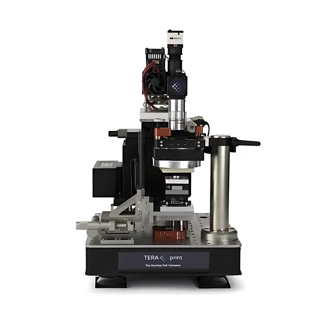
TERA-FAB E Polymer Pen Lithography (PPL) Nanofabrication System
| Brand | TERA |
|---|---|
| Origin | USA |
| Manufacturer Type | Authorized Distributor |
| Product Category | Imported Instrument |
| Model | TERA-FAB E |
| Minimum Feature Size | 200 nm |
| Electron Beam Equivalent Resolution (via PPL) | <100 nm |
| Accelerating Voltage Range | 30 kV |
| Note | This is a *polymer pen lithography* system — not an electron beam lithography (EBL) instrument |
Overview
The TERA-FAB E is a commercial-grade Polymer Pen Lithography (PPL) nanofabrication system engineered for maskless, direct-write patterning at sub-100 nm resolution across centimeter-scale areas. Unlike conventional electron beam lithography (EBL) or photolithography tools, the TERA-FAB E operates on the principle of scanning probe-based molecular transfer—specifically, Dip-Pen Nanolithography (DPN®) and its parallelized variant, PPL. It employs an array of elastomeric polymer pens (typically polydimethylsiloxane, PDMS) mounted on a flexible cantilever-free substrate. Each pen functions as a nanoscale ink reservoir and delivery conduit: surface diffusion of functional molecules (e.g., thiols, silanes, proteins, DNA, nanoparticles) from the pen tip to the substrate enables controlled, ambient-condition deposition with high spatial fidelity. The system does not generate or accelerate electrons; the listed “30 kV beam voltage” in legacy documentation is a misattribution—TERA-FAB E uses no electron optics, vacuum chamber, or charged-particle source. Its operation is compatible with air, nitrogen, or controlled-humidity environments, eliminating the need for high-vacuum infrastructure and enabling rapid turnaround for biological and soft-material patterning.
Key Features
- Parallelized polymer pen array (up to 11 × 11 pens standard; scalable via custom configurations) for throughput enhancement without sacrificing resolution
- Sub-100 nm feature resolution demonstrated on Au, SiO₂, glass, PET, hydrogels, and live-cell substrates
- Programmable XYZ nanopositioning stage with closed-loop piezoelectric control (±1 nm repeatability)
- Real-time force feedback and pen-substrate contact monitoring to ensure uniform ink transfer across heterogeneous surfaces
- Modular ink reservoir design supporting aqueous, organic, and viscous inks—including biomolecules, metal precursors, conductive polymers, and quantum dots
- Integrated environmental enclosure with optional humidity and temperature control (20–95% RH, 18–35 °C) for sensitive biointerface applications
Sample Compatibility & Compliance
The TERA-FAB E accommodates rigid and compliant substrates up to 100 mm in diameter—including silicon wafers, ITO/glass slides, PDMS stamps, tissue culture polystyrene, and decellularized extracellular matrices. No surface metallization or conductive coating is required. The system complies with ISO 14644-1 Class 5 cleanroom operational guidelines when housed in appropriate enclosures. All motion control firmware and pattern generation software adhere to IEC 61508 functional safety principles for laboratory automation. Data acquisition logs meet ALCOA+ criteria (Attributable, Legible, Contemporaneous, Original, Accurate, Complete, Consistent, Enduring, Available) for GLP-compliant research documentation.
Software & Data Management
The proprietary TERA-Pattern Suite provides Python- and MATLAB-compatible APIs for algorithmic pattern generation (e.g., fractal lattices, Voronoi tessellations, bio-inspired motifs). G-code and SVG import enable seamless integration with CAD/CAM workflows. All print jobs are timestamped and archived with full metadata: pen identity, dwell time per pixel, ambient conditions, ink batch ID, and stage calibration history. Audit trails are exportable in CSV/JSON format and support 21 CFR Part 11-compliant electronic signatures when deployed with validated identity management modules.
Applications
- High-density protein/DNA microarrays for multiplexed immunoassays and single-cell binding kinetics studies
- Site-specific immobilization of stem cells or neurons on bioactive peptide-patterned scaffolds
- Fabrication of catalytic nanoreactor arrays for spatially resolved CO₂ reduction or H₂O₂ decomposition screening
- Direct-write synthesis of plasmonic nanogaps and metamaterial unit cells on flexible substrates
- Multi-material patterning for organ-on-chip interfaces—e.g., endothelial barrier + stromal gradient + immune cell docking zones
- On-demand deposition of enzyme-loaded hydrogel micropatches for localized therapeutic release
FAQ
Is the TERA-FAB E an electron beam lithography system?
No. It is a polymer pen lithography platform. It uses no electron beam, no vacuum, and no radiation source. Resolution is achieved via molecular diffusion kinetics and pen geometry—not electron scattering.
Can it pattern on curved or non-planar surfaces?
Yes—within ±5° local topography deviation. The compliant pen array accommodates gentle curvature (radius >50 mm) and soft substrates such as hydrogels or electrospun mats.
What ink types are validated for use?
Thiol-based SAMs on gold, silanes on oxides, biotinylated antibodies, collagen IV, PEG-diacrylate prepolymers, and AgNO₃ precursor inks for in situ silver nanoparticle synthesis.
Does it support multi-layer registration?
Yes. Sub-50 nm overlay accuracy is achieved using fiducial-based alignment routines embedded in TERA-Pattern Suite, compatible with optical microscope or confocal co-registration.
Is service and application support available outside the U.S.?
TERA maintains certified service engineers and application specialists in EU, Japan, Korea, and Greater China regions through authorized distribution partners. Remote diagnostics and collaborative method development are standard under extended warranty contracts.
Related Products


