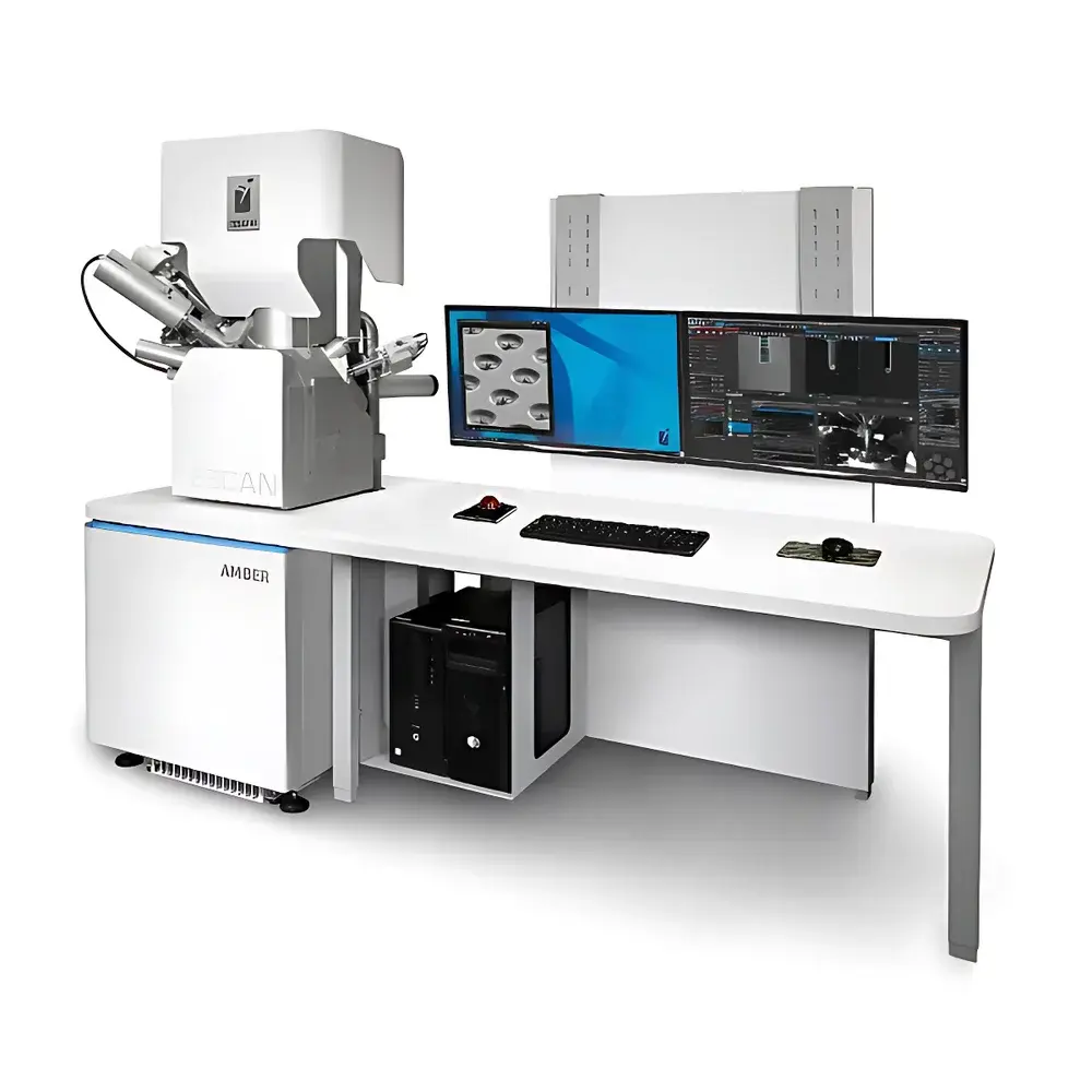
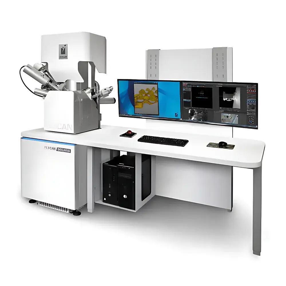
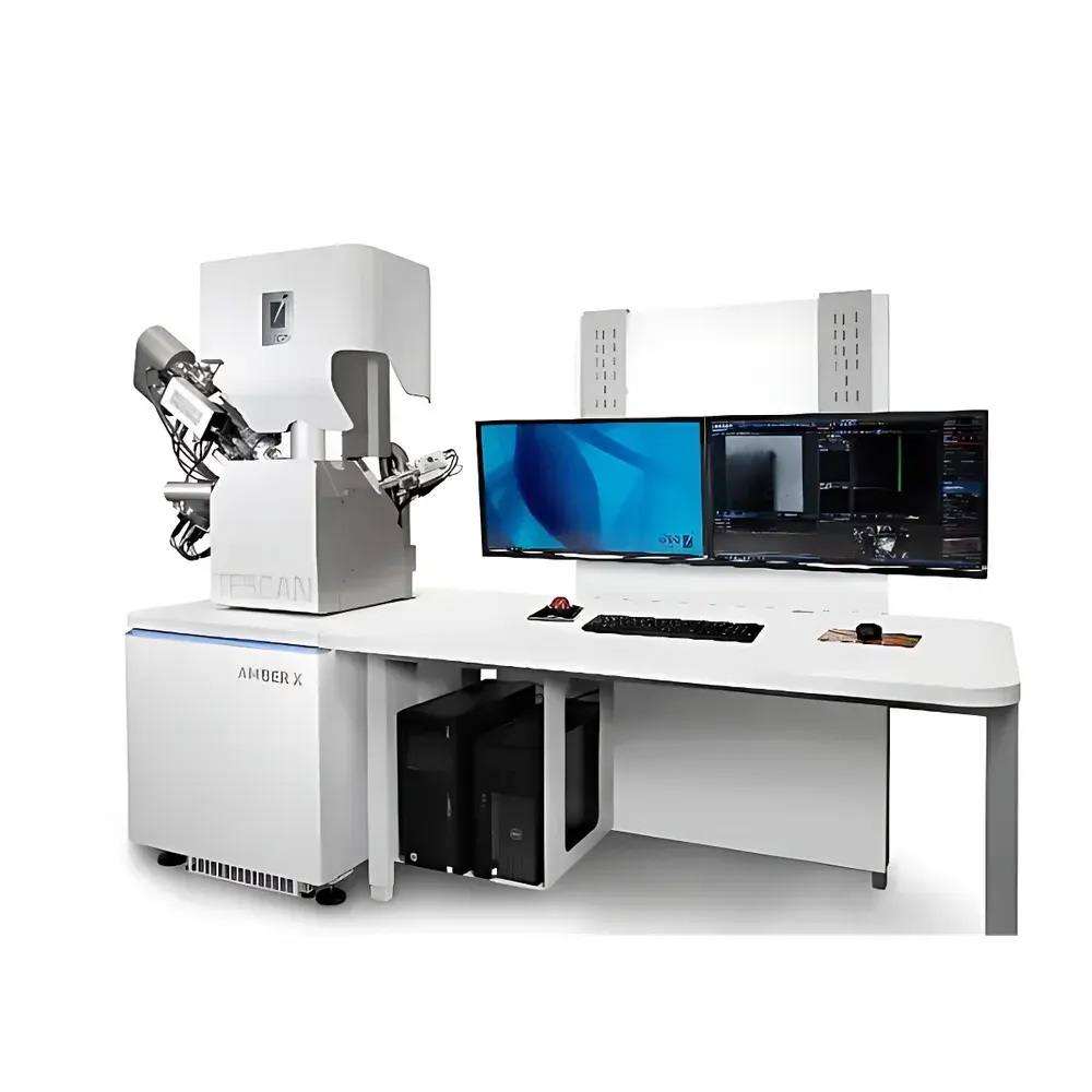
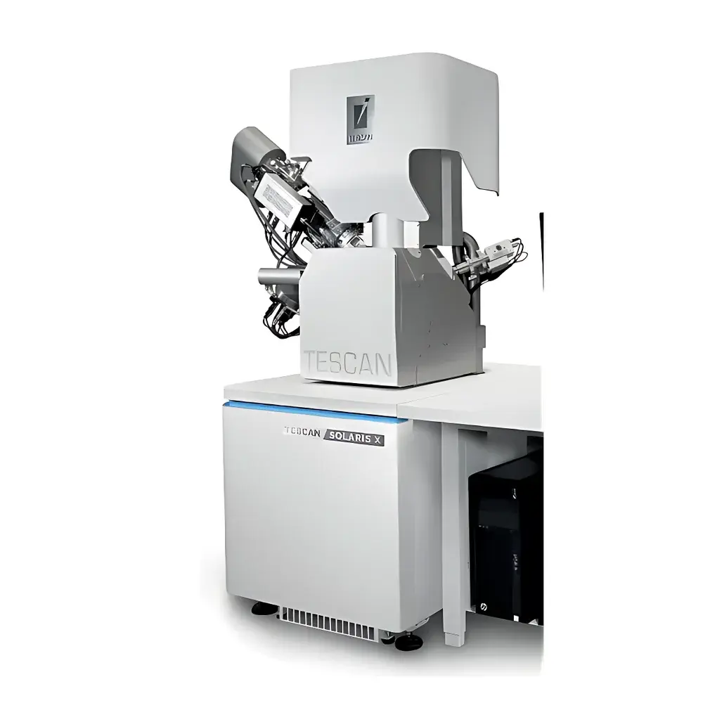
TESCAN AMBER / SOLARIS Series Plasma-FIB Dual-Beam Focused Ion Beam Scanning Electron Microscope
| Brand | TESCAN |
|---|---|
| Origin | Czech Republic |
| Model | AMBER / SOLARIS / AMBER X / SOLARIS X |
| Ion Sources | Liquid Metal Gallium (Ga⁺) & Xenon Plasma (Xe⁺) |
| Resolution (Xe-FIB) | <15 nm |
| Dual-Beam Alignment | Co-located Electron and Ion Probe Axes |
| Application Domain | Nanoscale Imaging, Cross-Sectioning, TEM Lamella Preparation, Circuit Edit, 3D Tomography, In Situ Nanofabrication |
Overview
The TESCAN AMBER and SOLARIS Series Plasma-FIB Dual-Beam Systems represent a class of high-performance focused ion beam scanning electron microscopes (FIB-SEM) engineered for nanoscale characterization, precision milling, and in situ analytical workflows. These instruments integrate two independent, co-registered beam columns — a thermally assisted field emission (Schottky) electron column for high-resolution SEM imaging and analysis, and a high-brightness ion column utilizing either liquid metal gallium (Ga⁺) or xenon plasma (Xe⁺) ion sources. Unlike conventional Ga-FIB systems limited by ion current and sputter rate, the Xe plasma ion source delivers up to 50× higher material removal rates while maintaining sub-15 nm probe resolution — enabling rapid, high-fidelity site-specific preparation of transmission electron microscopy (TEM) lamellae, semiconductor cross-sections, and 3D nanotomographic volumes. The precisely aligned electron and ion optical axes ensure real-time SEM monitoring during FIB milling, eliminating positional drift and enabling closed-loop nanofabrication with micron-level repeatability across multi-hour operations.
Key Features
- Co-registered dual-beam architecture with sub-100 nm beam coincidence tolerance across the full working distance range (4–25 mm)
- Dual ion source capability: High-stability Ga⁺ source for ultra-high spatial resolution (<5 nm SEM, <7 nm FIB) and Xe plasma source for high-current milling (up to 100 nA) with <15 nm resolution
- Integrated energy-dispersive X-ray spectroscopy (EDS), electron backscatter diffraction (EBSD), and cathodoluminescence (CL) detectors compatible with simultaneous FIB-SEM operation
- Automated lamella lift-out workflow with integrated micromanipulator and cryo-transfer option for TEM sample preparation under contamination-controlled conditions
- Advanced stage design with 5-axis motorized control (X/Y/Z/tilt/rotation), ±90° tilt range, and sub-nanometer step resolution for complex 3D reconstruction and serial sectioning
- Modular vacuum architecture featuring differential pumping stages, base pressure <1×10⁻⁷ Pa in SEM mode and <5×10⁻⁶ Pa in FIB mode
Sample Compatibility & Compliance
The AMBER/SOLARIS platforms accommodate conductive, semi-conductive, and insulating samples up to 150 mm in diameter (standard chamber) or 200 mm (optional large-chamber configuration). Conductive coating (e.g., carbon or platinum sputtering) is supported via integrated sputter coater module. For beam-sensitive biological or polymer specimens, low-voltage SEM imaging (0.1–5 kV) and cryogenic sample stages (−180 °C) are available as factory-installed options. All systems comply with IEC 61000-6-3 (EMC emissions), IEC 61000-6-2 (immunity), and CE Machinery Directive 2006/42/EC. Software audit trails, user access levels, and electronic signatures meet FDA 21 CFR Part 11 requirements when configured with TESCAN’s GLP/GMP-compliant software package. Routine operation adheres to ISO/IEC 17025 principles for accredited laboratories performing failure analysis or materials qualification.
Software & Data Management
TESCAN’s Unified Platform (UP) software provides a unified interface for instrument control, image acquisition, automated scripting (Python API), and 3D reconstruction. The FIB-SEM workflow engine supports fully automated serial sectioning, region-of-interest (ROI) targeting, and iterative feedback loops between imaging and milling steps. All acquired data — including SEM/FIB images, EDS maps, stage coordinates, beam parameters, and timestamps — are stored in vendor-neutral TIFF/HDF5 formats with embedded metadata compliant with FAIR (Findable, Accessible, Interoperable, Reusable) data principles. Raw datasets can be exported directly to third-party tomography tools (e.g., Avizo, Dragonfly, Thermo Fisher Velox) without proprietary lock-in. Audit logs record every user action, parameter change, and system event with ISO 8601 timestamps and SHA-256 checksums for traceability in regulated environments.
Applications
- Failure analysis in advanced semiconductor nodes (≤3 nm logic, GAA transistors, HBM stacks) via cross-sectional imaging and circuit edit
- Routine TEM lamella preparation from bulk materials, thin films, and battery electrodes with minimal curtaining and amorphization
- 3D nanotomography of porous media, catalysts, and composite microstructures using slice-and-view methodology
- In situ mechanical testing inside the chamber using nanoindenter or micro-tensile stages synchronized with FIB milling
- Site-specific extraction and transfer of quantum dots, nanowires, or 2D materials for correlative TEM/STEM analysis
- Development of photonic crystals, plasmonic metasurfaces, and MEMS devices requiring sub-20 nm feature definition and metrology
FAQ
What distinguishes Xe plasma FIB from conventional Ga⁺ FIB?
Xe plasma FIB offers significantly higher ion currents (up to 100 nA vs. typical Ga⁺ max of 20 nA) and faster milling rates while preserving <15 nm resolution — making it ideal for rapid bulk material removal without sacrificing final surface quality.
Can the system perform automated TEM lamella preparation?
Yes — TESCAN’s AutoLamella+ workflow automates lift-out, thinning, polishing, and final trimming with real-time SEM feedback and pre-programmed thickness monitoring via electron channeling contrast.
Is cryo-capability available for beam-sensitive samples?
Cryo-transfer systems and cold stages down to −180 °C are optional configurations, enabling high-fidelity imaging and milling of hydrated biological tissues, polymers, and lithium-based battery materials.
How is data integrity ensured in regulated industries?
With optional Part 11 compliance package, the system enforces role-based access control, electronic signatures, immutable audit trails, and data encryption — satisfying FDA, ISO 13485, and ICH-GCP requirements.
What maintenance intervals are recommended for Xe plasma source operation?
Xe plasma source lifetime exceeds 1,500 operational hours under standard conditions; source replacement and alignment are performed by certified field service engineers during scheduled preventive maintenance visits every 12 months.


