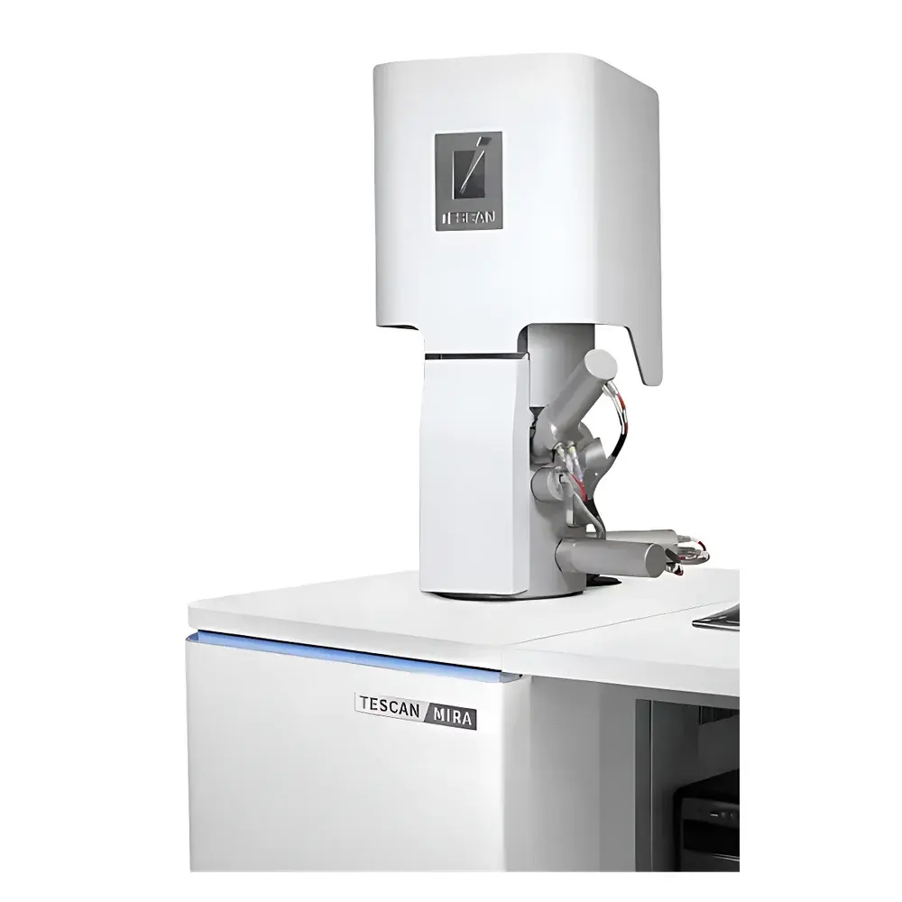
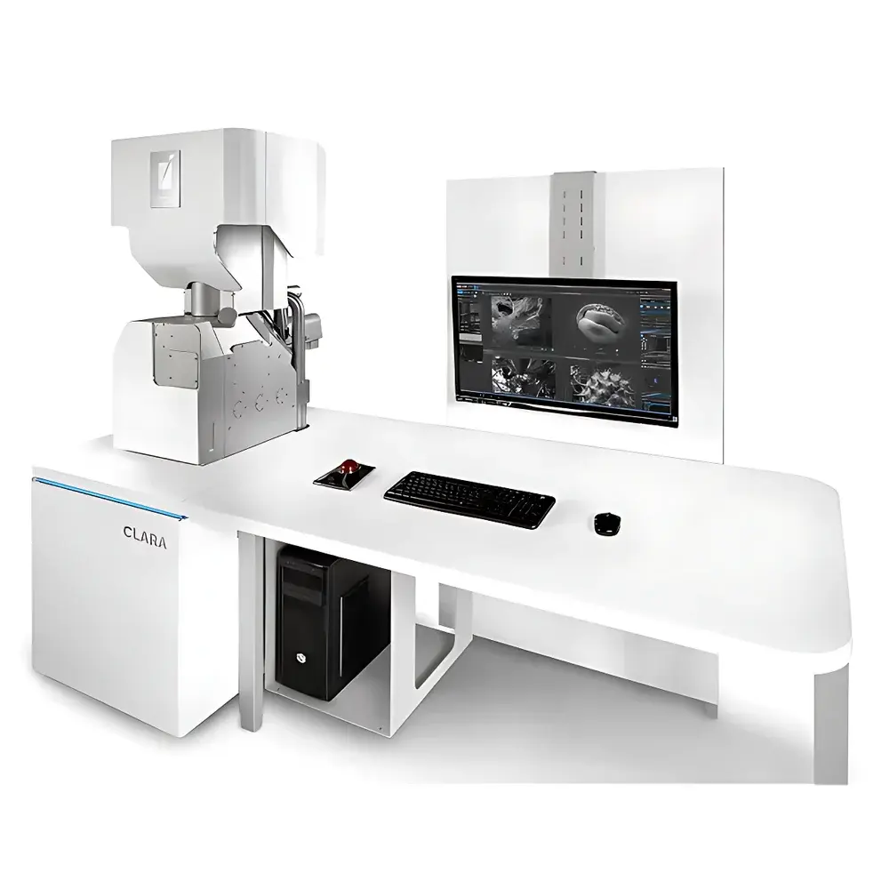
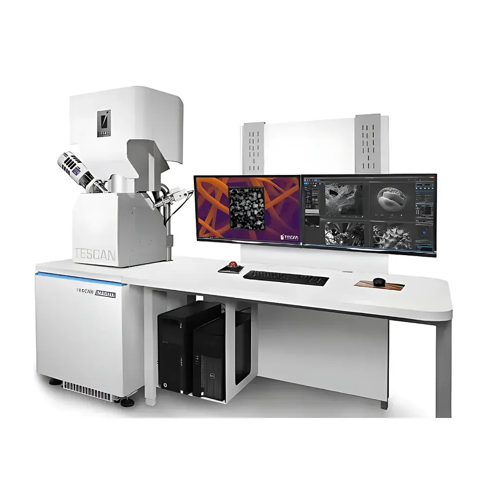
TESCAN MIRA / CLARA / MAGNA High-Resolution Field-Emission Scanning Electron Microscope
| Brand | TESCAN |
|---|---|
| Origin | Czech Republic |
| Model Series | MIRA / CLARA / MAGNA |
| Instrument Type | Floor-Standing FE-SEM |
| Electron Source | Schottky Field-Emission Gun |
| Beam Technology | BrightBeam (CLARA), Triglav Ultra-High-Resolution Column (MAGNA) |
| Application Scope | Nanoscale Imaging & Microanalysis of Conductive, Semi-Conductive, and Insulating Materials |
| Compliance Framework | Designed for ASTM E1558, ISO 16700, and GLP/GMP-aligned laboratory environments |
Overview
The TESCAN MIRA, CLARA, and MAGNA series represent a family of high-resolution field-emission scanning electron microscopes (FE-SEMs) engineered for nanoscale surface imaging, compositional analysis, and structural characterization across diverse scientific and industrial domains. These instruments operate on the fundamental principle of raster-scanning a focused electron beam across a solid specimen in vacuum, detecting secondary electrons (SE), backscattered electrons (BSE), and characteristic X-rays to generate topographic, atomic-number contrast, and elemental distribution data. Unlike thermionic sources, the Schottky field-emission electron gun delivers exceptional brightness, energy stability, and long-term emission consistency—enabling sub-nanometer resolution at low accelerating voltages (0.1–30 kV) while maintaining high signal-to-noise ratio and minimal sample charging. The platform supports variable pressure (VP) and low-vacuum modes for non-conductive or hydrated specimens without metal coating, making it suitable for routine QC, failure analysis, and exploratory research where fidelity and reproducibility are critical.
Key Features
- Three modular platform variants: MIRA (balanced performance for general-purpose nanoscale imaging), CLARA (BrightBeam™ electron optical column enabling zero-magnetic-field imaging for magnetic and beam-sensitive materials), and MAGNA (Triglav™ ultra-high-resolution column with optimized electron optics and multi-detector geometry for enhanced surface sensitivity and contrast).
- Integrated high-efficiency in-lens SE detector, through-the-lens BSE detector, and optional STEM-in-SEM transmission detector for simultaneous bright-field/dark-field imaging.
- Advanced stage design with 5-axis motorized control (X/Y/Z/tilt/rotation), precision repeatability ≤1 µm, and large travel range (150 × 150 × 60 mm) accommodating wafer-level samples and bulk geological specimens.
- Optional integrated energy-dispersive X-ray spectrometer (EDS), wavelength-dispersive spectrometer (WDS), electron backscatter diffraction (EBSD), and cathodoluminescence (CL) modules for correlative microstructural and chemical analysis.
- Intuitive user interface powered by TESCAN’s Unified Software Platform (USP), supporting automated workflows, scripting (Python API), and real-time image stitching over large areas (up to 100 mm²).
Sample Compatibility & Compliance
The TESCAN FE-SEM platforms accommodate a broad spectrum of specimen types—including conductive metals, semiconductors, ceramics, polymers, biological tissues, geological thin sections, and uncoated insulators—without compromising resolution or introducing artifacts. VP-SEM capability allows imaging of partially hydrated or outgassing samples at pressures up to 200 Pa, eliminating the need for sputter coating in many life science and environmental applications. All systems are designed and validated in accordance with international standards including ASTM E1558 (standard guide for SEM use in materials characterization), ISO 16700 (specifications for FE-SEM performance testing), and IEC 61000-6-3 (EMC compliance). For regulated environments, optional audit-trail logging, electronic signatures, and 21 CFR Part 11–compliant software modules are available to support FDA-regulated pharmaceutical development, medical device inspection, and GLP/GMP-compliant analytical laboratories.
Software & Data Management
TESCAN’s Unified Software Platform (USP) provides a unified environment for instrument control, acquisition, processing, and reporting. It features automated calibration routines, drift compensation algorithms, and batch-processing pipelines for high-throughput metrology tasks such as particle size distribution analysis (PSD), grain boundary mapping, and defect counting. Raw image data is stored in open-format TIFF or proprietary .tiff-based formats compatible with third-party analysis tools (e.g., ImageJ, MATLAB, Thermo Scientific Avizo). Metadata embedding includes full acquisition parameters (kV, probe current, dwell time, working distance, detector settings), stage coordinates, and timestamping—ensuring traceability and reproducibility. Networked deployment enables remote operation, centralized license management, and integration into enterprise LIMS or ELN infrastructures via RESTful API.
Applications
- Semiconductor & Microelectronics: Cross-sectional imaging of TSVs, BEOL interconnects, solder joint integrity, MEMS actuator morphology, and lithographic pattern fidelity at <1 nm resolution.
- Materials Science: Phase identification in multiphase alloys, porosity quantification in thermal barrier coatings, fracture surface analysis in composites, and nanoindentation site correlation.
- Life Sciences: Uncoated cell membrane topology, collagen fibril organization in decalcified bone, viral particle distribution on tissue sections, and cryo-SEM–compatible workflows with optional cryo-transfer stages.
- Earth & Environmental Sciences: Mineral phase mapping in polished rock mounts, microfossil ultrastructure, particulate matter morphology in air filters, and nanoparticle dispersion in soil matrices.
- Forensics & Failure Analysis: Fractography of fractured components, gunshot residue particle morphology, counterfeit IC package inspection, and adhesive bondline integrity assessment.
FAQ
What distinguishes the CLARA from the MAGNA platform?
The CLARA employs BrightBeam™ technology—a magnetic-free electron optical column—ideal for imaging ferromagnetic materials (e.g., permanent magnets, transformer cores) without beam deflection or image distortion. The MAGNA utilizes the Triglav™ column, optimized for ultimate surface sensitivity and contrast at low kV, particularly advantageous for beam-sensitive organics and uncoated insulators.
Can these systems perform EDS elemental mapping without sample coating?
Yes—when operated in low-vacuum or variable-pressure mode with appropriate charge compensation (e.g., gas ionization or beam deceleration), EDS mapping is feasible on non-conductive samples such as polymers, ceramics, or biological specimens without metallization.
Is remote operation supported for multi-site laboratories?
All models support secure remote access via TLS-encrypted VNC or dedicated client software, enabling real-time collaboration, training, and off-hours acquisition scheduling across geographically distributed facilities.
How is system calibration maintained over time?
TESCAN instruments include automated daily calibration routines for magnification, stigmation, and focus; optional traceable reference standards (e.g., NIST SRM 2090) and metrology-grade stage encoders ensure long-term dimensional accuracy compliant with ISO/IEC 17025 requirements.
Are there options for integrating machine learning–based image analysis?
Yes—the USP supports Python-based plugin architecture, allowing integration of custom AI models for automated feature detection (e.g., pore recognition, particle classification) and export to TensorFlow or PyTorch environments for model training and validation.


