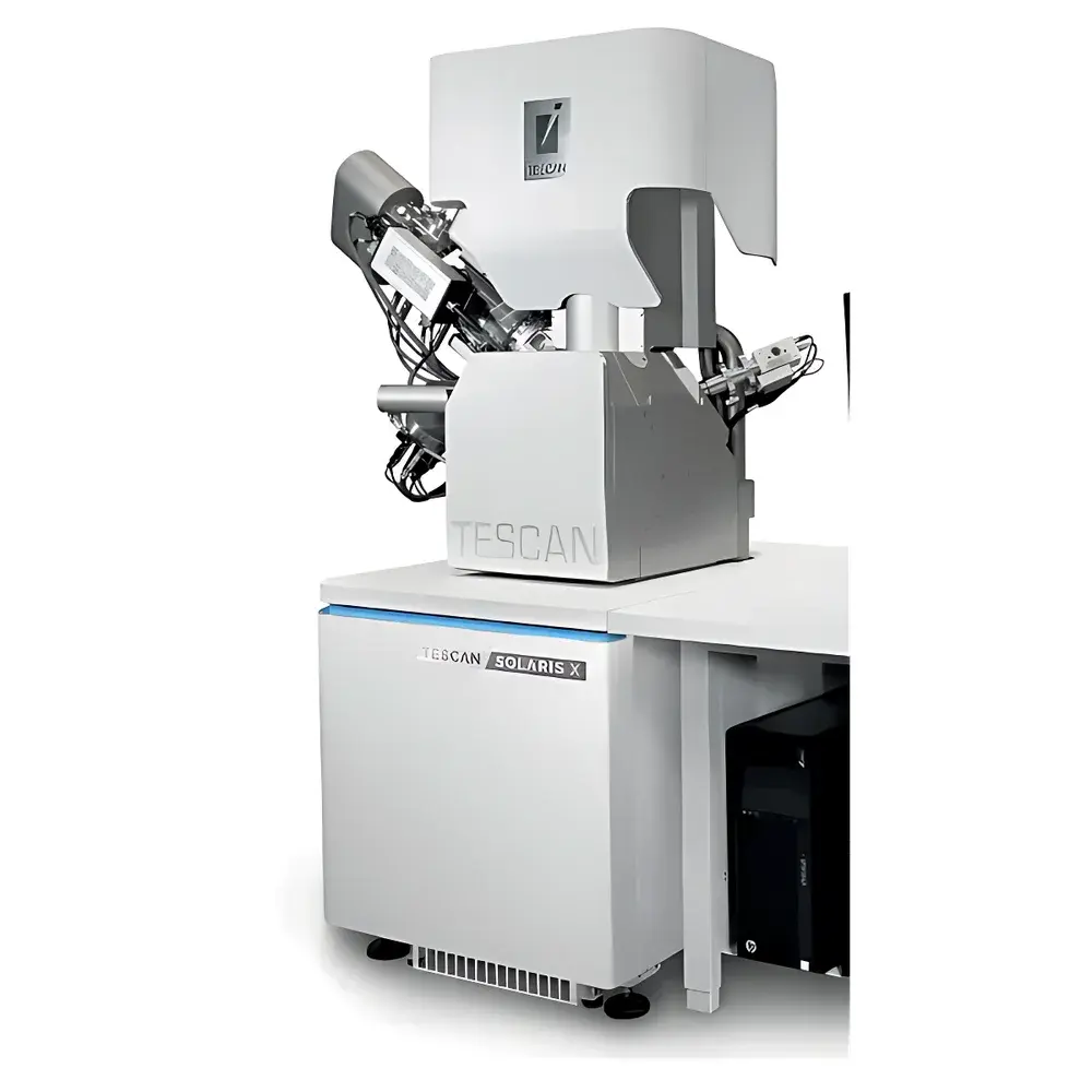
TESCAN SOLARIS X Xenon Plasma FIB-SEM DualBeam Microscope
| Brand | TESCAN |
|---|---|
| Origin | Czech Republic |
| Model | TESCAN SOLARIS X |
| Beam Type | Xenon (Xe⁺) Plasma Ion Source |
| SEM Column | Triglav™ UHR Schottky FE |
| FIB Column | iFIB+™ Xenon Plasma |
| Software Platform | TESCAN Essence™ |
| Detector System | TriSE™ + TriBE™ In-column SE/BSE |
| GIS Capacity | Up to 5 OptiGIS™ Units |
| Maximum FIB Current | 2 µA |
| FoV at 30 kV | >1 mm |
| Wafer Compatibility | 6″ and 8″ |
Overview
The TESCAN SOLARIS X is a high-performance xenon plasma dual-beam focused ion beam–scanning electron microscope (FIB-SEM) engineered for demanding physical failure analysis (PFA), 3D microstructural characterization, and precision nanofabrication in semiconductor, MEMS, advanced packaging, and optoelectronic device development. Unlike conventional gallium liquid-metal ion source (LMIS) FIB systems, the SOLARIS X employs a next-generation iFIB+™ xenon plasma ion column, delivering superior sputter yield, minimal subsurface damage, and negligible elemental contamination—critical for TEM lamella preparation, cross-sectioning of low-k dielectrics, and Ga-free compositional analysis. Its integrated Triglav™ ultra-high-resolution (UHR) Schottky field-emission SEM column provides sub-nanometer imaging resolution with exceptional surface sensitivity, enabled by energy-filtered axial backscattered electron (BSE) detection and multi-angle signal collection via TriSE™ and TriBE™ in-column detectors. The system operates on fundamental principles of electron–solid and ion–solid interactions: high-energy electrons generate secondary electrons (SE), backscattered electrons (BSE), and characteristic X-rays for topographic, compositional, and crystallographic mapping; while the focused Xe⁺ ion beam enables controlled material removal, deposition, and ion-induced secondary electron imaging—enabling correlative structural, chemical, and crystallographic analysis at the nanoscale.
Key Features
- Next-generation iFIB+™ xenon plasma ion column delivering up to 2 µA total ion current with stable, high-quality beam profiles—enabling rapid large-area milling (e.g., 1 mm-wide cross-sections in hours) without compromising spatial fidelity.
- Triglav™ UHR SEM column with optimized in-lens detector architecture, offering threefold improvement in signal detection efficiency and energy-selective BSE acquisition for enhanced surface contrast and topographic sensitivity.
- TriSE™/TriBE™ multi-detector system enabling simultaneous acquisition of multiple electron signals (SE, low-energy BSE, high-energy BSE) from distinct angular trajectories—facilitating material phase discrimination, grain boundary delineation, and charge contrast imaging.
- OptiGIS™ gas injection system—expandable to five independent channels or integrated 5-nozzle online manifold—for site-specific precursor delivery in etching, deposition, and selective enhancement (e.g., Pt/C deposition, XeF₂ isotropic etching, H₂O-based oxidation).
- DrawBeam™ vector scanning engine enabling sub-pixel beam positioning accuracy, real-time dwell time modulation, and deterministic pattern generation for electron-beam lithography and high-fidelity FIB milling.
- Piezo-driven aperture turret with 30 selectable apertures, enabling rapid switching between FIB current presets and minimizing downtime associated with manual alignment or aperture replacement.
- In-Flight Beam Tracing™ technology for dynamic optimization of electron probe size and current during analytical sessions—ensuring optimal conditions for EDS, WDS, and EBSD acquisition without sacrificing spatial resolution.
Sample Compatibility & Compliance
The SOLARIS X accommodates samples up to 200 mm in diameter—including full 6″ and 8″ wafers—with unrestricted access across the entire surface due to its 60° objective lens geometry and large-volume chamber design. It supports conductive, semi-conductive, and insulating specimens through integrated low-voltage imaging modes, beam deceleration, and charge compensation strategies. The platform meets requirements for regulated environments: instrument control logs, user-access audit trails, and session metadata recording align with GLP/GMP documentation practices; software architecture supports 21 CFR Part 11-compliant electronic signatures when deployed with validated Essence™ configuration. All vacuum, stage motion, and beam parameter settings are traceable and exportable for QA/QC reporting. No Ga⁺ ion interference ensures unambiguous TOF-SIMS spectra and eliminates spectral overlap with elements such as Ce, Ge, and Ga—making it suitable for failure root-cause analysis in advanced node ICs where trace elemental quantification is critical.
Software & Data Management
TESCAN Essence™ serves as the unified software platform governing all hardware subsystems—including SEM/FIB imaging, GIS control, stage navigation, automated workflows, and correlative data fusion. Its modular architecture includes application-specific wizards (e.g., Cross-section Auto-Setup, TEM Lamella Prep, 3D Tomography Acquisition) that guide users through complex sequences with real-time feedback and adaptive parameter adjustment. All acquired datasets—including SE/BSE images, EDS maps, EBSD patterns, and FIB milling logs—are stored in vendor-neutral HDF5 format with embedded metadata (beam energy, dwell time, stage coordinates, gas flow rates). Post-processing pipelines support voxel-based 3D reconstruction, phase segmentation, porosity analysis, and crystallographic orientation mapping using integrated tools or export to third-party platforms (e.g., Avizo, Thermo Scientific Velox, Oxford AZtec). Remote operation and multi-user session management are supported via secure TLS-encrypted client-server architecture.
Applications
- Physical failure analysis of advanced packaging structures: TSVs, microbumps, RDLs, and fan-out wafer-level packages—leveraging Ga-free Xe⁺ milling to preserve interfacial chemistry and prevent artifact formation.
- 3D microstructural tomography of solder joints, battery electrodes, and metal matrix composites—enabled by synchronized FIB milling and EDS/EBSD acquisition at each slice.
- TEM specimen preparation for cryo-EM and in-situ TEM studies—where minimal amorphization, no implanted Ga, and controllable thinning kinetics are essential.
- Nanoscale circuit edit and maskless prototyping using DrawBeam™-driven vector FIB milling and electron-beam-induced deposition (EBID).
- High-throughput metrology of EUV photomasks, nanoimprint templates, and photonic crystals—utilizing large-field stitching and automated defect review protocols.
- TOF-SIMS depth profiling of ultra-thin gate stacks and 2D material heterostructures—free from Ga⁺ background interference and compatible with sub-10 nm lateral resolution.
FAQ
What distinguishes xenon plasma FIB from traditional Ga⁺ FIB?
Xenon ions exhibit significantly lower nuclear stopping power and reduced interaction volume compared to Ga⁺, resulting in less lattice disorder, shallower implantation depth, and no residual metallic contamination—critical for TEM sample integrity and quantitative surface analysis.
Can the SOLARIS X perform simultaneous EDS and EBSD during FIB tomography?
Yes—its synchronized acquisition architecture allows concurrent collection of EDS spectra and EBSD patterns at each milling step, enabling true 3D compositional and crystallographic reconstruction.
Is the system compatible with existing laboratory LIMS or ELN infrastructure?
Essence™ supports standardized data export formats (HDF5, TIFF, CSV) and RESTful API endpoints for integration with enterprise laboratory informatics systems.
How does the iFIB+™ column achieve high current without beam degradation?
Through advanced plasma confinement optics, multi-stage beam shaping, and active thermal stabilization of the extraction electrode—maintaining sub-10 nm probe size even at 1 µA ion current.
What wafer handling options are available for production-integrated PFA labs?
Optional load-lock modules with cassette-to-chamber transfer, robotic end-effectors, and SECS/GEM protocol support enable seamless integration into automated fab metrology workflows.


