TFT Parameter Testing System McScience T5000
| Brand | McScience |
|---|---|
| Origin | South Korea |
| Manufacturer Type | Authorized Distributor |
| Origin Category | Imported |
| Model | T5000 |
| Pricing | Available Upon Request |
Overview
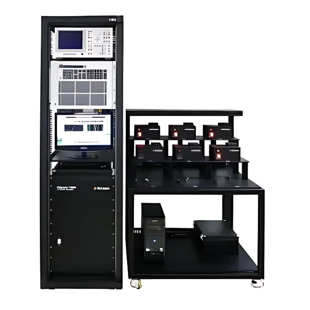
The McScience T5000 TFT Parameter Testing System is a precision semiconductor characterization platform engineered for the electrical evaluation of thin-film transistor (TFT) devices under controlled bias, thermal, and optical stress conditions. Utilizing a high-accuracy source-measure unit (SMU) architecture with synchronized voltage sourcing and current/voltage measurement capabilities, the system implements standard four-terminal (Kelvin) probing methodology to eliminate lead resistance errors and ensure traceable, low-noise DC parameter extraction. Designed specifically for R&D laboratories and process development teams in display, flexible electronics, and emerging oxide/organic semiconductor industries, the T5000 supports full IDS–VGS and IDS–VDS transfer and output curve acquisition, enabling quantitative extraction of fundamental device physics parameters critical to material qualification and process optimization.
Key Features
- Modular multi-channel configuration supporting up to 16 independent SMU channels (expandable via optional hardware modules), enabling parallel testing of discrete TFTs or array-based substrates
- Dual-mode operation: Standard static DC characterization mode and accelerated stress testing modes—including thermal stress (temperature-controlled chamber interface, −40 °C to +150 °C) and photostress (integrated LED or broadband lamp source with calibrated irradiance control)
- Automated parameter extraction engine compliant with IEEE Std 1620.1–2018 (Standard for Semiconductor Device Parameter Extraction) for consistent calculation of μFE, μsat, Vth, SS, Ion/Ioff, and subthreshold swing
- Programmable pulse bias capability (pulse width: 10 µs–10 s; duty cycle adjustable) for transient response analysis and contact resistance de-embedding
- Hardware-level synchronization between voltage sources, current measurements, environmental controllers, and optical stimuli—ensuring temporal fidelity during stress-correlated measurements
- Front-panel touchscreen interface with intuitive test flow builder and real-time waveform preview, complemented by remote control via TCP/IP and SCPI command set
Sample Compatibility & Compliance
The T5000 accommodates standard semiconductor wafer formats (up to 200 mm) and rigid/flexible substrate configurations including glass, silicon, polyimide, and PET. Probe station integration supports both manual micropositioning and semi-automated XYZ stages with optical alignment assistance. All measurement protocols adhere to industry-standard definitions outlined in JEDEC JEP184 (TFT Characterization Guidelines) and ISO/IEC 17025–2017 requirements for calibration traceability. The system supports GLP-compliant audit trails, user-access-level authentication, and electronic signature functionality aligned with FDA 21 CFR Part 11 for regulated environments.
Software & Data Management
The embedded T5000 Control Suite provides a unified environment for test sequence definition, real-time data visualization, and post-acquisition analysis. Raw measurement data is stored in HDF5 format with embedded metadata (timestamp, environmental conditions, instrument configuration, operator ID). Batch analysis tools enable statistical evaluation across device arrays—including spatial mapping of mobility uniformity, threshold voltage shift (ΔVth) distribution, and lifetime extrapolation using Arrhenius or Eyring models. Export options include CSV, MATLAB .mat, and industry-standard SPICE model parameter files (.mod). Software validation documentation (IQ/OQ protocols) and version-controlled release notes are provided for GMP-aligned deployments.
Applications
- Characterization of amorphous-silicon (a-Si), low-temperature polycrystalline silicon (LTPS), indium gallium zinc oxide (IGZO), and other metal-oxide TFTs for active-matrix OLED and LCD backplane development
- Electrical reliability assessment of organic TFTs (OTFTs) under combined thermal–light stress, supporting ISO 11341 (artificial weathering) and IEC 61215 (photovoltaic module qualification) derived test profiles
- Process window qualification in thin-film deposition and annealing steps—correlating film morphology (via SEM/XRD cross-reference) with extracted μFE and SS values
- Accelerated aging studies for flexible electronics, including bending-cycle-dependent parameter drift quantification using programmable mechanical actuator interfaces
- Device modeling support: extraction of compact model parameters (e.g., BSIM-IMG, PSP) for TCAD simulation and circuit-level verification
FAQ
What types of TFT technologies does the T5000 support?
The system is validated for a-Si, LTPS, IGZO, ZnO, pentacene, P3HT, and other solution-processed or vacuum-deposited channel materials.
Can the T5000 perform time-resolved measurements such as bias-stress stability tests?
Yes—it supports continuous monitoring over hours/days with configurable logging intervals (100 ms to 10 min), automatic Vth tracking via constant-current method, and drift rate calculation per JEDEC JESD245.
Is the software compatible with third-party data analysis platforms like Python or MATLAB?
Yes—the system provides native API access via RESTful web services and direct HDF5 file structure documentation for seamless integration into custom analysis pipelines.
Does the T5000 meet international calibration and traceability standards?
All SMU modules are factory-calibrated against NIST-traceable references; calibration certificates and uncertainty budgets are supplied with each unit.
How is probe contact resistance minimized during low-current measurements?
The system employs guarded Kelvin sensing, auto-zeroing offset compensation, and selectable filtering bandwidths (1 Hz to 10 kHz) to maintain signal integrity below 1 pA resolution.


