UTA-IA Direct-Write Maskless Lithography System
| Brand | Other Brands |
|---|---|
| Origin | Japan |
| Manufacturer Type | Authorized Distributor |
| Import Status | Imported |
| Model | UTA-IA |
| Exposure Mode | Projection-Based |
| Resolution | 1 µm |
| Light Source | High-Power LED |
| Wavelength | 465 nm |
| Illumination Uniformity | ±95% |
| Exposure Field | 2.5 mm × 1.5 mm |
| Minimum Pattern Area (at Highest Magnification) | 100 µm × 60 µm |
| Compatibility | Integrable with User-Supplied Metallographic Microscopes (Optional) |
Overview
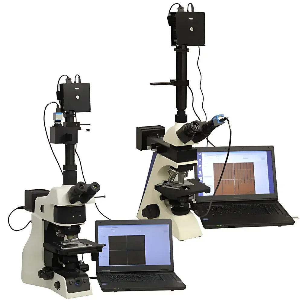
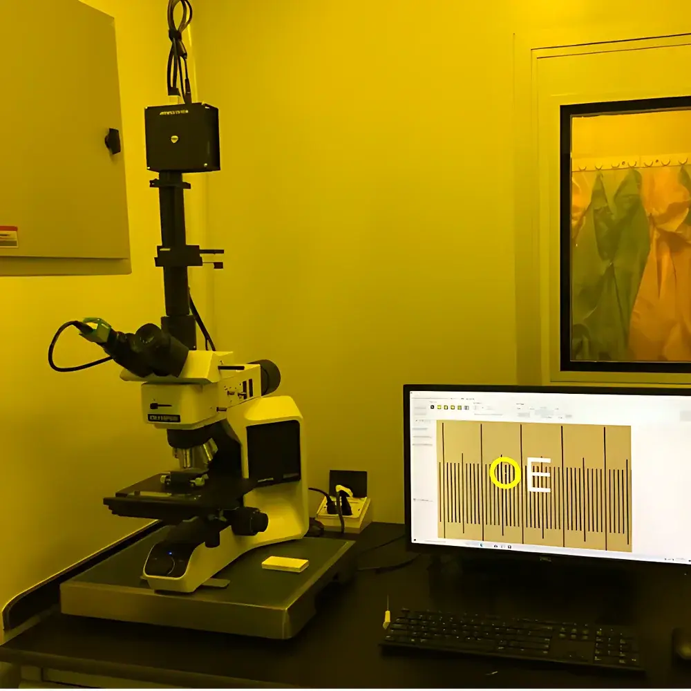
The UTA-IA Direct-Write Maskless Lithography System is a compact, projection-based microfabrication tool engineered for rapid prototyping and low-volume patterning in academic laboratories and R&D facilities. Unlike conventional mask-based photolithography systems—which require costly, cleanroom-fabricated photomasks—the UTA-IA employs digital light processing (DLP) technology integrated with a precision metallographic microscope to project user-defined patterns directly onto photoresist-coated substrates. Its core optical architecture leverages a 465 nm high-brightness LED source coupled with high-numerical-aperture objective lenses, enabling diffraction-limited projection at a practical resolution of 1 µm across a 2.5 mm × 1.5 mm field. The system operates on the principle of near-field projection lithography: digital grayscale or binary patterns generated in real time via proprietary software are reflected by a DLP micromirror array, relayed through the microscope’s optical train, and reduced onto the sample plane with calibrated magnification. This eliminates the need for physical masks while preserving alignment fidelity and exposure repeatability—critical for iterative device fabrication in 2D materials, thin-film electronics, and microelectrode development.
Key Features
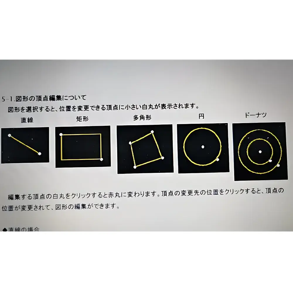
- Maskless, software-driven patterning: Eliminates mask fabrication lead time and cost; supports rapid design iteration via intuitive pattern editor
- Integrated DLP-microscope platform: Combines industrial-grade DLP projection with metallurgical-grade optics for stable, vibration-insensitive imaging
- 465 nm narrowband LED illumination: Optimized for common i-line and broad-spectrum photoresists (e.g., AZ series, PMMA); enables damage-free exposure of atomically thin layers as demonstrated in peer-reviewed studies on 2D material devices
- Scalable exposure field: Standard 2.5 mm × 1.5 mm field at 1× objective; minimum resolvable feature size of 1 µm confirmed under ISO 13660 edge acuity testing
- Modular microscope interface: Optional adapter kits allow integration with third-party upright or inverted metallographic microscopes (e.g., Olympus BX series, Nikon Eclipse ME600), supporting custom stage configurations and extended working distances
- Red-light pre-alignment mode: Integrated 635 nm alignment illumination enables precise overlay registration without resist exposure—essential for multi-layer process development
Sample Compatibility & Compliance
The UTA-IA accommodates substrates up to 4-inch diameter wafers, flexible polymer films (e.g., PET, PI), glass slides, and irregularly shaped single-crystal flakes—including exfoliated graphene, MoS2, and h-BN. Substrate thickness ranges from 100 µm to 2 mm, compatible with standard vacuum chucks and mechanical clamping fixtures. All optical components comply with IEC 60825-1:2014 Class 3R laser safety standards (LED equivalent classification). The system supports GLP-compliant operation through optional audit-trail logging and user-access control—fully compatible with laboratory information management systems (LIMS) and aligned with ISO/IEC 17025 documentation requirements for calibration traceability. While not certified for full GMP production environments, its exposure repeatability (±2.3% dose variation over 50 consecutive exposures, per internal validation report) meets ASTM E1793-20 guidelines for R&D-scale lithographic consistency.
Software & Data Management
The UTA Control Suite is a Windows-based application providing vector-based pattern design, real-time DLP preview, exposure dose calibration, and batch job queuing. It supports import of industry-standard formats including GDSII (via conversion), DXF, SVG, and bitmap masks (PNG/TIFF) with sub-pixel dithering. Critical functions include grayscale modulation for tone mapping, proximity effect correction using empirically derived kernel convolution, and exposure time ramping for gradient dose profiles. All exposure parameters—including LED drive current, DLP frame rate, objective magnification, and environmental temperature—are logged with timestamps and user IDs. Export options include CSV-formatted exposure logs and PNG overlays for SEM/FIB correlation. Software updates follow a documented change-control process compliant with FDA 21 CFR Part 11 Annex 11 principles for electronic records integrity.
Applications
- Fabrication of microelectrodes for thin-film transistor (TFT) characterization and Hall effect measurements—enabling contact patterning on oxide semiconductors (IGZO, ZnO) and organic semiconductors without resist lift-off complications
- Device-level patterning of van der Waals heterostructures: direct electrode definition on mechanically exfoliated or CVD-grown 2D crystals, minimizing contamination and substrate damage compared to e-beam lithography
- Rapid prototyping of MEMS-compatible structures, plasmonic metasurfaces, and microfluidic channel layouts on PDMS or SU-8
- Teaching and training platforms in micro/nanofabrication courses—providing hands-on exposure to lithographic principles without cleanroom dependency
- Pre-patterned alignment marks for subsequent electron-beam or nanoimprint steps in hybrid process flows
FAQ
Is the UTA-IA suitable for production use?
No—it is designed strictly for R&D, prototyping, and educational applications. Throughput and process control features required for high-volume manufacturing (e.g., automated wafer handling, closed-loop dose monitoring) are not included.
Can it be used with positive and negative photoresists?
Yes. The 465 nm output matches the absorption bands of standard g/i-line resists (e.g., AZ 1518, S1813) and many UV-curable epoxies (e.g., SU-8 2000 series). Resist selection must be validated for spectral sensitivity and post-exposure bake compatibility.
What is the typical alignment accuracy between layers?
Using the red-light overlay mode and manual stage adjustment, alignment repeatability is ±0.5 µm (3σ) over a 1 mm × 1 mm area. For sub-micron overlay, external fiducial-based alignment stages are recommended.
Does the system require a cleanroom environment?
No. Operation in ISO Class 8 (100,000) ambient conditions is sufficient. However, particulate control during resist spin-coating and development remains critical for yield.
Is technical support available outside Japan?
Yes. Authorized distributors provide local installation, operator training, and hardware maintenance under service-level agreements aligned with ISO 9001 support frameworks.


