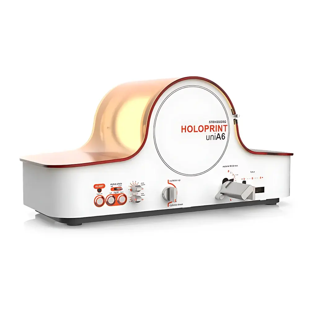
UV-Curable Nanoimprint Lithography System uni A6
| Origin | Denmark |
|---|---|
| Manufacturer Type | Distributor |
| Origin Category | Imported |
| Model | uni A6 |
| Price Range | USD 70,000 – 112,000 |
Overview
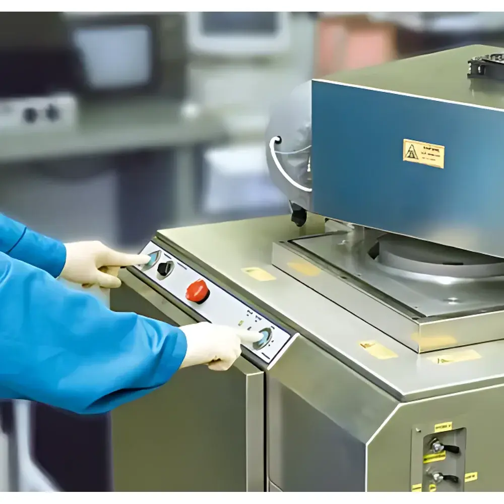
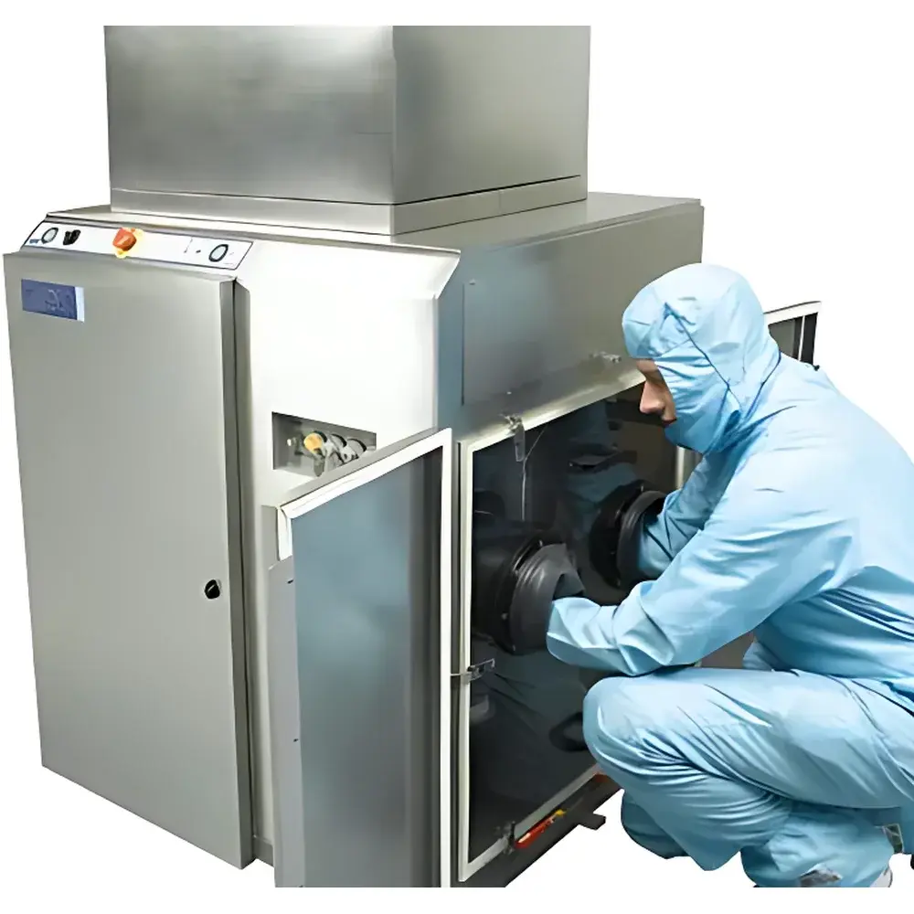
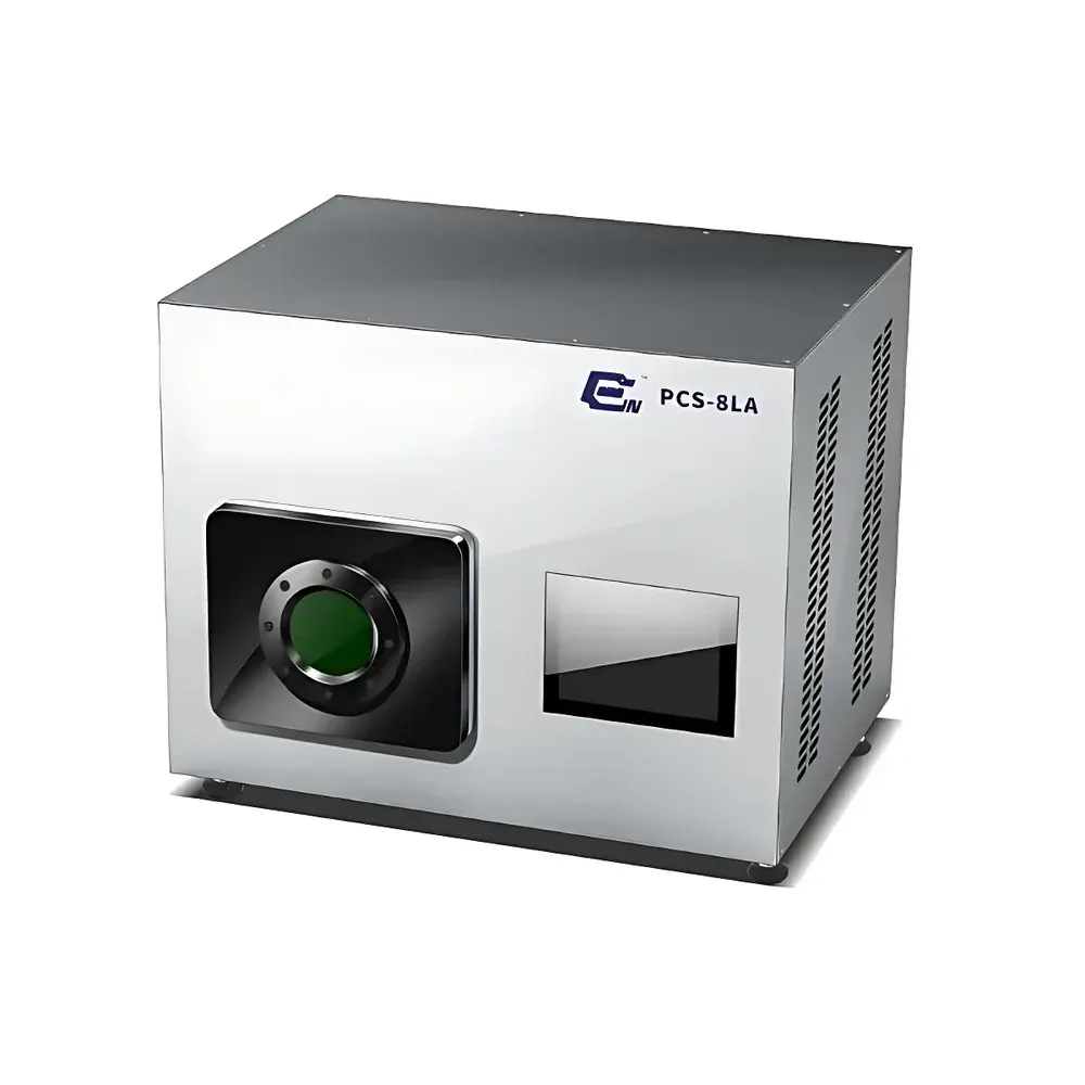
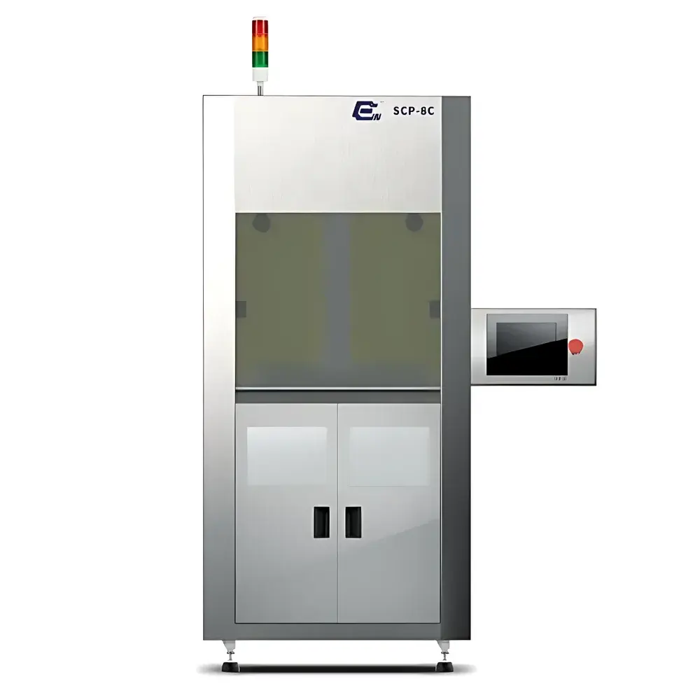
The uni A6 UV-Curable Nanoimprint Lithography System is a benchtop roll-to-plate (R2P) nanoimprint platform engineered for high-fidelity, scalable replication of micro- and sub-100 nm surface topographies. Unlike conventional photolithography or electron-beam lithography—both limited by throughput, cost, and substrate compatibility—the uni A6 leverages contact-mode thermal and UV-assisted imprinting to transfer nanoscale patterns from durable polymer stamps onto diverse substrates with nanometer-level fidelity. Its core operating principle relies on precise mechanical alignment, controlled pressure application (0.1–10 bar), and broadband UV-LED irradiation (365 nm peak, 10–500 mW/cm² adjustable intensity) to initiate rapid (<5 s) photocuring of acrylate- or epoxy-based resists. Designed specifically for semiconductor R&D labs, photonics prototyping facilities, and advanced materials development teams, the system bridges the gap between lab-scale nanofabrication and pilot-line manufacturability—enabling deterministic pattern transfer without vacuum chambers, high-energy radiation sources, or cleanroom-grade infrastructure.
Key Features
- Proprietary European-patented R2P (Roll-to-Plate) imprint architecture for repeatable, low-defect pattern transfer across rigid and flexible substrates
- Integrated high-uniformity UV optical engine with real-time irradiance monitoring and closed-loop dose control
- Substrate agnostic capability: compatible with silicon wafers, glass, PET, PI, metal foils, and curved or textured surfaces
- Feature size range: 20 nm minimum line/space resolution up to 100 µm macrostructures—validated via SEM and AFM metrology
- Modular thermal control stage (25–120 °C) for hybrid UV/thermal imprint processes and residual layer thickness optimization
- Automated alignment system with <100 nm overlay accuracy using dual-camera vision and motorized theta-Z compensation
- Low-force imprint mechanism (<50 N total load) minimizing template deformation and extending stamp lifetime beyond 30,000 cycles
Sample Compatibility & Compliance
The uni A6 supports imprinting on substrates ranging from 25 mm × 25 mm up to 150 mm × 150 mm (customizable to 200 mm square). It accommodates both hard (Si, quartz, sapphire) and soft (PET, PEN, PDMS) substrates with thicknesses from 50 µm to 5 mm. All fluidic and optical components comply with IEC 61000-6-3 (EMC emissions) and IEC 61000-6-2 (immunity). The UV exposure module meets IEC 62471 Photobiological Safety classification (Risk Group 2), and full operational logs—including pressure, temperature, UV dose, and alignment data—are timestamped and exportable for GLP/GMP audit trails per FDA 21 CFR Part 11 requirements.
Software & Data Management
Controlled via uniLITH™ v4.2 software (Windows 10/11 x64), the system provides intuitive workflow management—from recipe setup and process parameter logging to real-time force/dose feedback and post-process defect mapping. All parameters are stored in encrypted SQLite databases with user role-based access (admin/operator/viewer). Raw sensor data (pressure transducers, thermocouples, UV radiometers) are sampled at 1 kHz and archived with metadata compliant with ASTM E2500-22 (Standard Guide for Specification, Design, and Verification of Pharmaceutical and Biopharmaceutical Manufacturing Systems). Export formats include CSV, HDF5, and vendor-neutral XML for integration into LIMS or MES platforms.
Applications
- Diffractive optical elements (DOEs) and security holograms for banknote and ID card anti-counterfeiting
- Nanotextured light-trapping surfaces for silicon and perovskite solar cells (enhancing Jsc by >15% in validated prototypes)
- Polymer waveguide arrays and AR/VR grating couplers with <0.5 dB/cm propagation loss
- Superhydrophobic/superhydrophilic functional surfaces for lab-on-chip microfluidics and point-of-care diagnostics
- Plasmonic metasurfaces for biosensing (LSPR shift >10 nm per 1 ng/mm² biomolecule adsorption)
- Photonic crystal templates for colloidal self-assembly and quantum dot patterning
- Hard-mask fabrication for anisotropic etching of Si, GaN, and Al₂O₃ via reactive ion etching (RIE)
FAQ
What is the minimum feature size achievable with the uni A6?
The system consistently replicates features down to 20 nm half-pitch under optimized resist and template conditions, verified by cross-sectional SEM and critical dimension AFM.
Can the uni A6 imprint on curved or non-planar substrates?
Yes—its adaptive conformal pressure system enables imprinting on substrates with radii of curvature ≥25 mm, including cylindrical lenses and wearable electronics substrates.
Is the system compatible with standard NIL resists such as mr-NIL210 or Optool UV-NIL?
All commercially available UV-curable nanoimprint resists—including those from Micro Resist Technology, DOW, and Shin-Etsu—are fully supported via customizable cure profiles.
Does the uni A6 support automated template cleaning or inspection?
While not integrated, the system includes standardized mounting interfaces and vacuum ports compatible with third-party template inspection stations (e.g., EVG’s IQ Aligner) and plasma ashers (e.g., Diener Zepto).
What level of training and technical support is provided?
Installation qualification (IQ), operational qualification (OQ), and comprehensive operator certification (8 hours onsite + remote follow-up) are included; extended service contracts cover preventive maintenance, calibration, and software updates for up to 5 years.