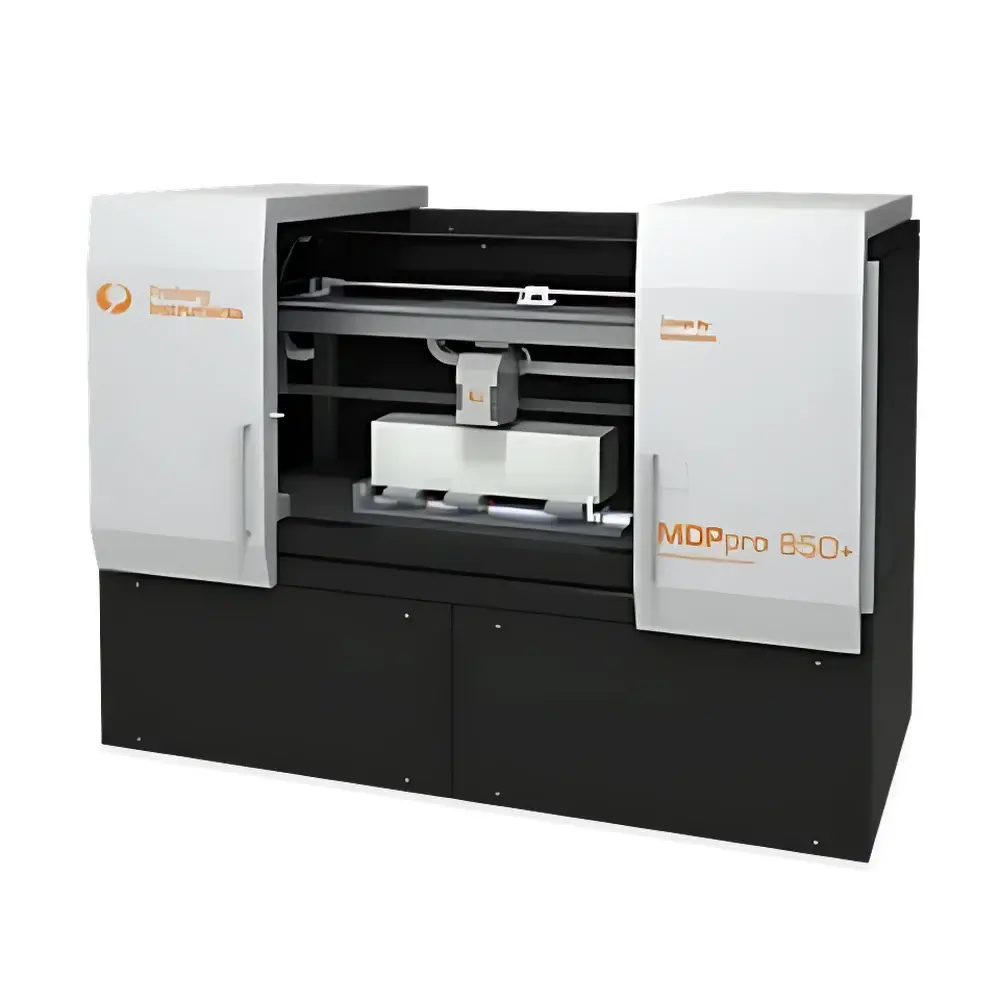
Freiberg Instruments MDPpro 850+ µPCD/MDP Minority Carrier Lifetime Tester
| Brand | Freiberg Instruments |
|---|---|
| Origin | Germany |
| Model | MDPpro 850+ |
| Measurement Principle | Microwave Photoconductance Decay (µPCD) & Quasi-Steady-State Photoconductance (QSS-PCD/MDP) |
| Lifetime Range | 20 ns – 100 ms (for resistivity > 0.3 Ω·cm) |
| Scan Speed | Line scan < 30 s |
| Simultaneous Parameters | Minority carrier lifetime (µPCD/MDP), photoconductivity, resistivity |
| Sample Geometry Recognition | Automatic (G12, M10 bricks, wafers up to Ø300 mm) |
| Laser Sources | 980 nm IR diode (≤500 mW) + 905 nm IR diode (≤9 W) |
| Resistivity Range | 0.5 – 5 Ω·cm (custom ranges available) |
| Conductivity Type | p-type and n-type silicon |
| Compliance | SEMI PV9-1110, CE, ISO 9001 |
| Software Platform | MDP Studio (Windows 11+, .NET Framework, dual Ethernet) |
| Power Supply | 100–250 V AC, 6 A |
| Dimensions (W×H×L) | 2560 × 1910 × 1440 mm |
| Weight | ~200 kg |
Overview
The Freiberg Instruments MDPpro 850+ is a high-precision, non-contact microwave photoconductance decay (µPCD) and quasi-steady-state photoconductance (QSS-PCD/MDP) system engineered for quantitative minority carrier lifetime characterization of crystalline silicon materials across the photovoltaic and semiconductor value chain. It operates on the physical principle of transient or steady-state photoconductance monitoring following optical excitation: when an IR laser pulse or continuous-wave beam generates excess carriers in silicon, the resulting change in microwave absorption (µPCD mode) or conductance (MDP/QSS mode) is measured with sub-microsecond temporal resolution. This enables direct extraction of effective minority carrier lifetime (τeff), photoconductivity (Δσ), and sheet resistance—without requiring ohmic contacts, surface passivation, or thermal processing. Designed specifically for inline and offline quality assurance in solar cell manufacturing, the MDPpro 850+ supports full-process monitoring—from Czochralski ingot slicing and brick sawing through wafering and cell processing—delivering traceable, reproducible data aligned with SEMI PV9-1110 requirements for lifetime metrology in PV production.
Key Features
- Simultaneous dual-mode measurement: µPCD (transient decay analysis) and MDP/QSS (quasi-steady-state photoconductance), enabling comprehensive recombination kinetics assessment under varying injection levels.
- Integrated resistivity mapping via four-point probe-compatible geometry recognition—no manual calibration required for G12, M10, or standard wafer formats (up to Ø300 mm).
- Automated sample geometry detection and stage alignment, reducing operator dependency and minimizing setup time between batch runs.
- Dual-wavelength IR excitation (980 nm and 905 nm) with independent power control (≤500 mW and ≤9 W, respectively), supporting depth-resolved lifetime profiling and iron contamination quantification in p-type Si.
- High-speed scanning architecture: line scans completed in under 30 seconds; full-area lifetime/resistivity maps acquired in less than 5 minutes at 1 mm spatial resolution.
- Rugged industrial enclosure (CE-certified, ISO 9001-manufactured) with integrated vibration damping, suitable for cleanroom or factory-floor deployment.
Sample Compatibility & Compliance
The MDPpro 850+ is validated for monocrystalline silicon ingots (125 × 125 mm² to 210 × 210 mm² cross-section), bricks up to 850 mm in length, and wafers up to Ø300 mm. It accommodates both p-type and n-type conductivity types and operates reliably across a resistivity range of 0.5–5 Ω·cm (extended ranges available upon request). All measurements adhere to SEMI standard PV9-1110 for lifetime metrology in photovoltaics, ensuring compatibility with international quality gate criteria for HJT, TOPCon, PERC+, bifacial PERC, and perovskite-silicon tandem cell production. The system’s hardware and software architecture support audit-ready operation under GLP/GMP-aligned workflows, including user access control, electronic signatures, and full measurement traceability—enabling compliance with FDA 21 CFR Part 11 where required.
Software & Data Management
MDP Studio—the proprietary Windows-based control and analysis platform—provides a modular, role-based interface compliant with modern laboratory informatics standards. It features hierarchical user management with operator, engineer, and administrator privileges; configurable test recipes with parameter locking and version history; real-time visualization of transient decay curves and QSS response; and export of calibrated lifetime, photoconductivity, and resistivity matrices in HDF5, CSV, and TIFF formats. Advanced analysis modules include iron concentration mapping (via lifetime vs. injection-level modeling), trap density estimation (using temperature-dependent lifetime spectroscopy protocols), and LBIC (light-beam induced current) correlation overlays. Remote IP-based access allows secure off-site diagnostics, software updates, and technical support—minimizing instrument downtime without compromising data security.
Applications
- Process-critical lifetime mapping of silicon ingots to identify slip dislocations, oxygen precipitate bands (OSF rings), and crystal growth defects.
- In-line iron contamination screening in p-type Cz-Si wafers—correlating τeff degradation with Fei concentration at sub-ppt detection limits.
- Quantitative evaluation of emitter sheet resistance and bulk lifetime uniformity in TOPCon and HJT precursors—supporting junction optimization without destructive contact formation.
- Injection-dependent lifetime analysis to distinguish Shockley-Read-Hall recombination centers from Auger and radiative mechanisms—essential for passivation layer development.
- Trap energy level and density profiling using variable-temperature MDP measurements—enabling defect engineering in high-efficiency cell architectures.
- Multi-parameter qualification of multicrystalline and quasi-mono silicon bricks prior to wafering, identifying low-lifetime regions for yield optimization.
FAQ
What is the difference between µPCD and MDP/QSS measurement modes?
µPCD measures the transient decay of photoconductivity after a short laser pulse, yielding lifetime values under low-injection conditions. MDP (QSS-PCD) uses continuous illumination to determine steady-state photoconductivity, enabling injection-level-dependent lifetime analysis and resistivity mapping.
Can the system measure iron concentration directly?
Yes—through calibrated lifetime vs. injection-level modeling in p-type silicon, the MDPpro 850+ quantifies interstitial iron (Fei) concentration with sub-ppt sensitivity, traceable to ASTM F1531 reference methods.
Is the system compatible with automated factory environments?
It supports SECS/GEM communication protocols via Ethernet, integrates with MES systems through OPC UA, and offers barcode-triggered recipe loading for unattended operation.
Does the software meet regulatory requirements for electronic records?
MDP Studio includes ALCOA+ compliant audit trails, electronic signatures, and 21 CFR Part 11–ready configuration options—including role-based access, immutable log files, and periodic integrity verification.
Can it characterize materials other than silicon?
The core µPCD/MDP methodology is optimized for crystalline silicon. While some GaAs or SiC samples may yield measurable signals, no factory calibration or application support is provided outside monocrystalline and multicrystalline Si.


