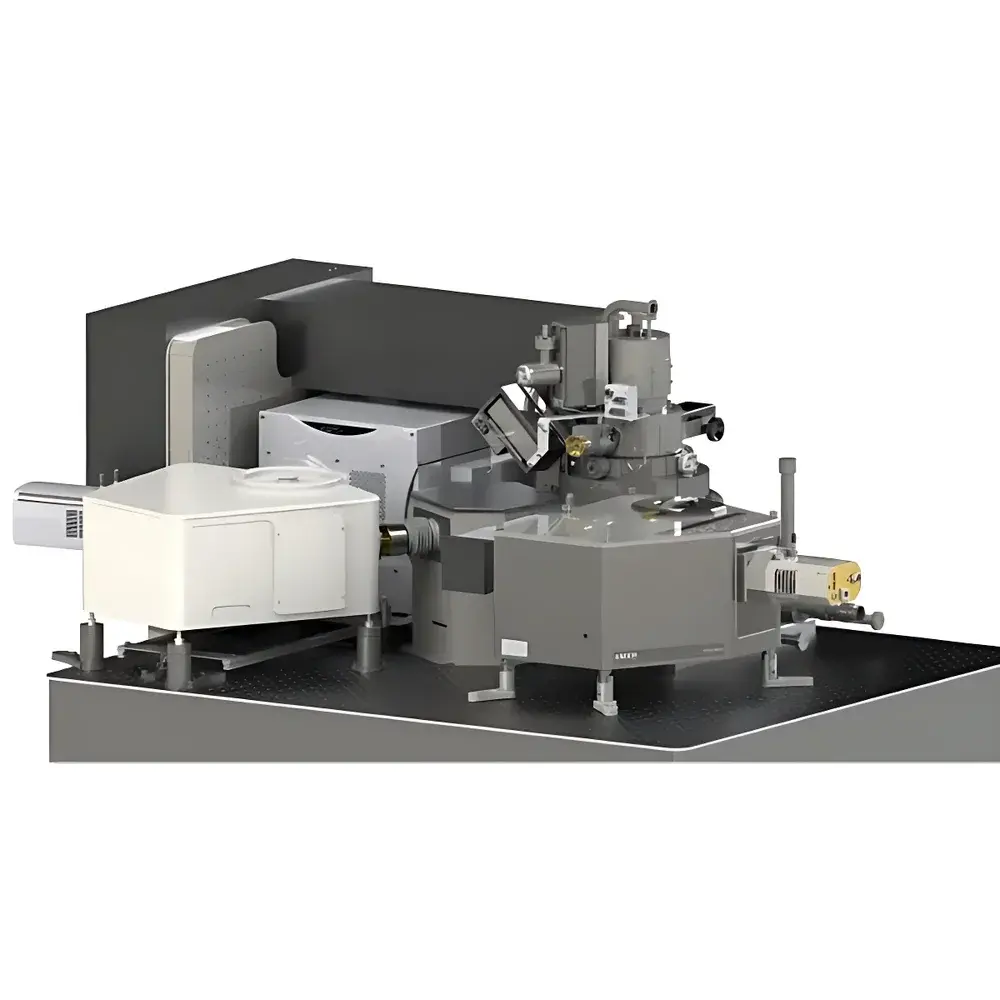
Attolight Allalin Quantitative Cathodoluminescence CL-SEM System
| Brand | Attolight |
|---|---|
| Origin | Switzerland |
| Model | Allalin |
| Electron Source | Schottky thermal field emission gun |
| Beam Energy Range | 1–10 keV |
| Minimum Probe Size | 3 nm @ 10 kV |
| Working Distance | 3 mm |
| Field of View | up to 300 µm |
| Optical NA | 0.71 (f/0.5) |
| Spectral Range | 200–1700 nm |
| Spectral Acquisition Speed | >900 spectra/s (UV-Vis), >180 spectra/s (NIR) |
| EBIC Current Detection Limit | 100 fA |
| Temperature Range (Cryostat) | 10 K to 300 K |
| Positioning Precision | 1 nm step, 100 nm repeatability over full range |
| Vacuum System | Ion pump (electron column) + turbomolecular pump (sample chamber) |
| Data Export Format | HDF5, TIFF, CSV |
| Software Compliance | Audit-trail enabled, metadata-embedded, GLP/GMP-ready |
Overview
The Attolight Allalin Quantitative Cathodoluminescence (CL) CL-SEM System is a fully integrated nanoscale spectroscopic platform that co-localizes high-resolution scanning electron microscopy (SEM) with quantitative cathodoluminescence imaging and spectroscopy. Unlike conventional CL systems—where optical collection efficiency, spectral calibration drift, and geometric misalignment between SEM and optical axes compromise quantification—the Allalin is engineered from the ground up for absolute photon flux calibration. Its core innovation lies in the monolithic integration of a high-numerical-aperture (NA = 0.71), achromatic reflective objective (180 nm – 1.6 µm) directly into the SEM column, ensuring precise focal plane alignment between electron probe and optical detection path. This eliminates parallax-induced artifacts and enables true quantitative CL mapping across fields up to 300 µm without sacrificing SEM resolution or signal fidelity. The system operates on the principle of electron-beam-induced photon emission from semiconductors and dielectrics, where emitted photons are collected with near-Lambertian efficiency (30% extraction uniformity across FOV) and dispersed via a motorized triple-grating spectrometer (320 mm focal length). Quantitative CL—defined as spectral intensity traceable to absolute photon counts per solid angle per incident electron—enables direct comparison across samples, instruments, and laboratories.
Key Features
- Simultaneous acquisition of high-resolution SEM topography, quantitative CL hyperspectral maps (512 × 512 pixels), and EBIC signals—all synchronized at pixel level
- Schottky field-emission electron source delivering stable beam currents from 30 pA to 300 nA, with sub-3 nm probe size at 10 kV
- Dual-detector spectral architecture: back-illuminated CCD (200–1100 nm, >900 spectra/s) and InGaAs array (600–1700 nm, >180 spectra/s), enabling seamless UV–NIR coverage
- Ultra-low-noise EBIC electronics with 100 fA current detection limit, gain range 10⁴–10¹⁵ V/A, and 100 kHz bandwidth
- 6-axis nanometric positioning stage (25 mm X/Y, 3 mm Z, ±3° tilt, ±10° rotation) with 1 nm step resolution and ≤100 nm repeatability over full travel
- Cryogenic sample environment: closed-cycle cryostat (10 K–300 K), digital temperature controller (±0.1 K stability), and <300 nm thermal drift/hour at 10 K
- Oil-free vacuum architecture: getter ion pump for electron column + turbomolecular pump for sample chamber; typical sample exchange time <20 min
Sample Compatibility & Compliance
The Allalin accommodates standard 3-inch SEM stubs and custom holders compatible with low-temperature operation. Its optical path supports transmission, reflection, and cross-sectional CL geometries. The system meets essential requirements for regulated environments: all measurement parameters—including dwell time, beam energy, detector gain, grating position, and slit width—are logged with timestamps and user IDs in immutable HDF5 containers. Metadata embedding complies with ASTM E2821-22 (Standard Guide for CL Data Reporting) and supports FDA 21 CFR Part 11 audit trails when deployed under validated SOPs. Instrument calibration certificates (wavelength, intensity, spatial) are traceable to NIST standards. The vacuum architecture satisfies ISO 20484:2017 (cleanliness classification for analytical electron microscopes).
Software & Data Management
Control is executed via a touch-enabled GUI optimized for rapid workflow navigation: real-time SEM/CL/EBIC overlay, intuitive region-of-interest definition, and live spectrum preview during acquisition. The software supports semi-automatic routines—including auto-focus, auto-stigmation, and beam alignment—reducing operator dependency. All raw data (images, spectra, stage coordinates, instrument settings) are saved concurrently in open, non-proprietary formats (HDF5, TIFF, CSV). Attolight’s Attomap analysis suite provides advanced tools for bandgap mapping, defect density quantification (e.g., threading dislocation counting via CL contrast modeling), strain extraction from peak shift analysis, and dopant profiling using donor–acceptor pair luminescence ratios. Remote access is secured via TLS-encrypted HTTP with role-based authentication and session timeout enforcement.
Applications
- Semiconductor process development: Quantitative mapping of GaN threading dislocation density, SiC basal plane defects, and AlGaN compositional gradients with <10 nm spatial registration accuracy
- Fault isolation in IC failure analysis: Correlation of electrical leakage paths (via EBIC) with localized non-radiative recombination centers (via CL quenching) at device-level resolution
- Nanophotonics characterization: Resonance mode identification in photonic crystal cavities and plasmonic nanostructures through momentum-resolved CL spectroscopy
- 2D material heterostructure analysis: Strain and interlayer twist angle determination via Raman-CL multimodal correlation
- Quantum emitter localization: Sub-10 nm precision positioning of single-photon sources (e.g., hBN defects, WSe₂ trions) using centroid-fitting on calibrated CL point-spread functions
- Geological and mineralogical studies: Trace-element distribution mapping in zircon and quartz via rare-earth-activated CL signatures
FAQ
What distinguishes quantitative CL from conventional CL?
Quantitative CL delivers spectrally calibrated photon counts per incident electron, eliminating instrument-dependent variables (e.g., collection efficiency drift, grating efficiency variation) through hardware-integrated calibration and fixed optical geometry.
Can Allalin perform time-resolved CL measurements?
The base system supports pulsed electron beams via optional picosecond laser-driven electron gun (Chronos module); lifetime-resolved CL requires external TCSPC hardware interfacing through TTL synchronization ports.
Is the system compatible with existing SEM infrastructure?
Allalin is a turnkey, self-contained CL-SEM platform—not an add-on kit—and requires dedicated floor space, vibration-isolated foundation, and independent power/cooling utilities.
How is spectral calibration maintained across long-term operation?
Wavelength calibration uses internal Hg/Ar lamp references acquired before each session; intensity calibration relies on NIST-traceable silicon photodiode standards measured during factory commissioning and verified annually.
Does the software support batch processing of hyperspectral datasets?
Yes—Attomap includes Python API bindings and CLI tools for scripted processing pipelines, including PCA decomposition, cluster analysis, and automated defect annotation using user-defined spectral thresholds.