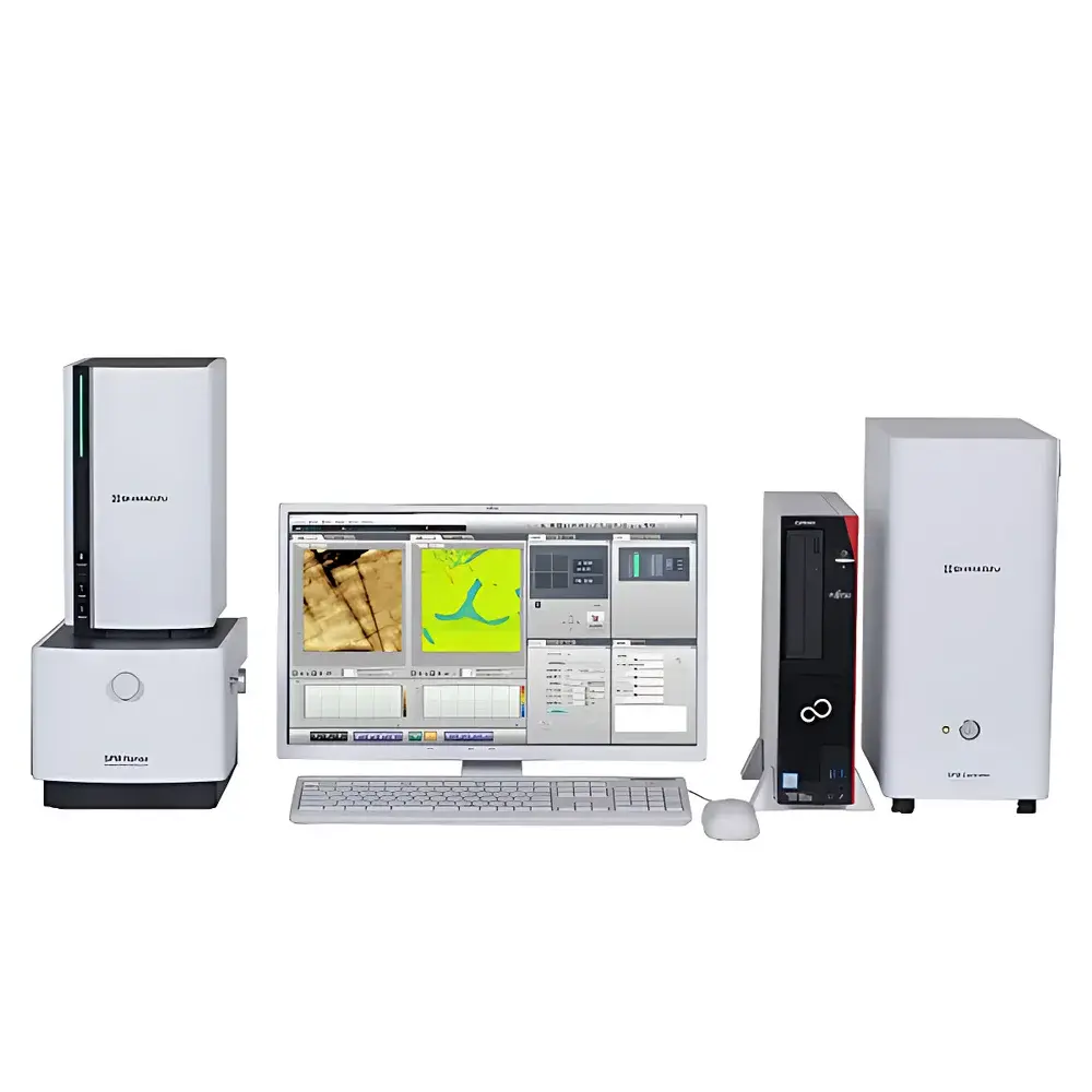


Shimadzu SPM-Nanoa Atomic Force Microscope
| Brand | Shimadzu |
|---|---|
| Origin | Japan |
| Model | SPM-Nanoa |
| Instrument Type | Material-oriented AFM |
| Position Detection Noise | < 0.02 nm (RMS) |
| Sample Diameter | 50 mm |
| Sample Thickness | ≤ 8 mm |
| XY Stage Travel Range | 5 × 5 mm |
Overview
The Shimadzu SPM-Nanoa is a high-performance, material-oriented atomic force microscope engineered for precision nanoscale topographic and mechanical characterization in academic research laboratories, industrial R&D centers, and quality control environments. Operating on the fundamental principle of dynamic (tapping) and contact-mode AFM, the SPM-Nanoa employs a laser beam deflection detection system coupled with a low-noise photodetector to transduce cantilever deflection into quantitative surface height data. Its sub-ångström vertical resolution—enabled by position detection noise below 0.02 nm (RMS)—supports reliable measurement of atomic steps, thin-film roughness, polymer domain structures, and nanostructured coatings. Designed explicitly for operational accessibility without compromising metrological integrity, the SPM-Nanoa integrates hardware-level stability enhancements—including a rigid optical baseplate, passive vibration isolation, and thermal drift compensation—with intelligent software-assisted workflows to reduce dependency on expert operator intervention.
Key Features
- Intelligent Automation Suite: “Automatic Observation” mode initiates full scan sequence—including probe approach, setpoint optimization, and image acquisition—via single-button execution; “Link On” performs real-time optical-to-SPM coordinate registration and automatic laser alignment; “NanoAssist” dynamically optimizes gain, integral time, and drive amplitude based on initial surface feedback.
- High-Fidelity Imaging Architecture: Dual-channel 16-bit DAC/ADC electronics support up to 8192 × 8192 pixel (8K) raster acquisition; integrated high-magnification optical microscope (10×–100×) enables precise region-of-interest navigation with sub-micron overlay accuracy between optical and SPM frames.
- Enhanced Acquisition Efficiency: Proprietary high-speed piezoelectric scanner achieves scan rates up to 4 Hz at 512 × 512 pixels; Nano 3D Mapping Fast algorithm accelerates large-area 3D reconstruction by >80% compared to conventional point-by-point interpolation methods.
- Modular Probe Handling System: Quick-release probe holder allows tool-free cantilever exchange in under 60 seconds; integrated tip-scan calibration routine validates lateral and vertical scaling prior to each session.
- Thermally Stable Platform: All-metal sample stage with integrated temperature monitoring; closed-loop XY positioning ensures repeatability better than ±2 nm over 5 × 5 mm range, even during multi-hour acquisitions.
Sample Compatibility & Compliance
The SPM-Nanoa accommodates standard conductive and non-conductive specimens up to 50 mm in diameter and 8 mm in thickness—including wafers, polished metals, ceramics, polymers, biological substrates (e.g., mica-supported lipid bilayers), and coated optical components. Its open-sample design permits in situ electrical biasing, liquid-cell operation (with optional fluid cell kit), and ambient or inert-gas environmental control. The system complies with ISO/IEC 17025 requirements for calibration traceability and supports GLP/GMP-aligned documentation through audit-trail-enabled software logging. Data files conform to standardized formats (e.g., WSxM, Gwyddion-compatible .spm) and include embedded metadata for instrument configuration, environmental conditions, and user identity—facilitating regulatory review per FDA 21 CFR Part 11 when deployed in pharmaceutical or medical device development.
Software & Data Management
Shimadzu’s NanoStation software (v4.2+) provides a unified interface for instrument control, real-time image processing, and quantitative analysis. Core modules include cross-sectional profiling, power spectral density (PSD) computation, grain size distribution mapping, adhesion force histogramming, and phase contrast deconvolution. All processing steps are scriptable via Python API, enabling integration into automated QA/QC pipelines. Raw data is stored in encrypted, timestamped project archives with version-controlled parameter snapshots. Software validation documentation—including IQ/OQ protocols and electronic signature capability—is available upon request for regulated environments.
Applications
- Surface metrology of semiconductor wafers and MEMS devices per ASTM E2226 and ISO 25178 standards
- Nanomechanical property mapping (modulus, adhesion, dissipation) of battery electrode composites and solid electrolytes
- Thin-film morphology analysis in OLED and perovskite photovoltaic R&D
- Characterization of self-assembled monolayers (SAMs), block copolymer nanodomains, and biomolecular arrays
- Failure analysis of microcracks, delamination, and interfacial defects in aerospace-grade composites
FAQ
Is the SPM-Nanoa compatible with third-party cantilevers?
Yes—the system supports standard 12.7 mm × 3.4 mm rectangular and triangular cantilevers from Bruker, Nanoworld, Olympus, and other ISO-compliant manufacturers.
Does the system support force spectroscopy modes?
Yes—force-distance curve acquisition, force-volume mapping, and PeakForce Tapping®-compatible modes are enabled via optional NanoMech module.
Can the SPM-Nanoa be operated in liquid or controlled atmosphere?
Liquid-cell imaging is supported with Shimadzu’s LFM-100 fluid cell accessory; environmental chamber integration (N₂, Ar, or vacuum) requires custom mounting and is available under engineering consultation.
What training and service options are provided?
Shimadzu offers on-site installation qualification (IQ), operator certification workshops, annual preventive maintenance contracts, and remote diagnostics with SLA-backed response times.
Is raw data export compliant with institutional data management policies?
All acquired datasets export in vendor-neutral HDF5 and ASCII formats; metadata fields adhere to the FAIR principles (Findable, Accessible, Interoperable, Reusable) and integrate with institutional LIMS platforms via RESTful API.


