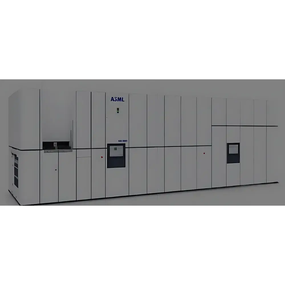
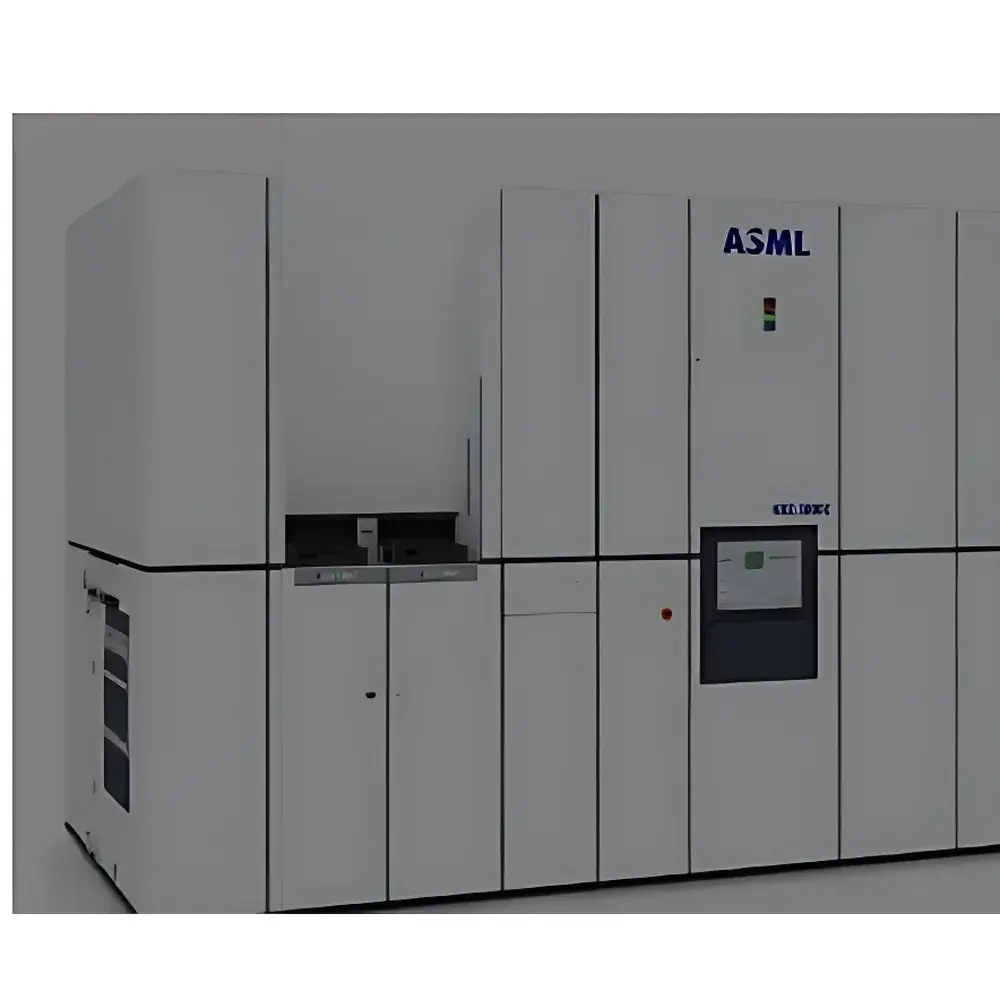
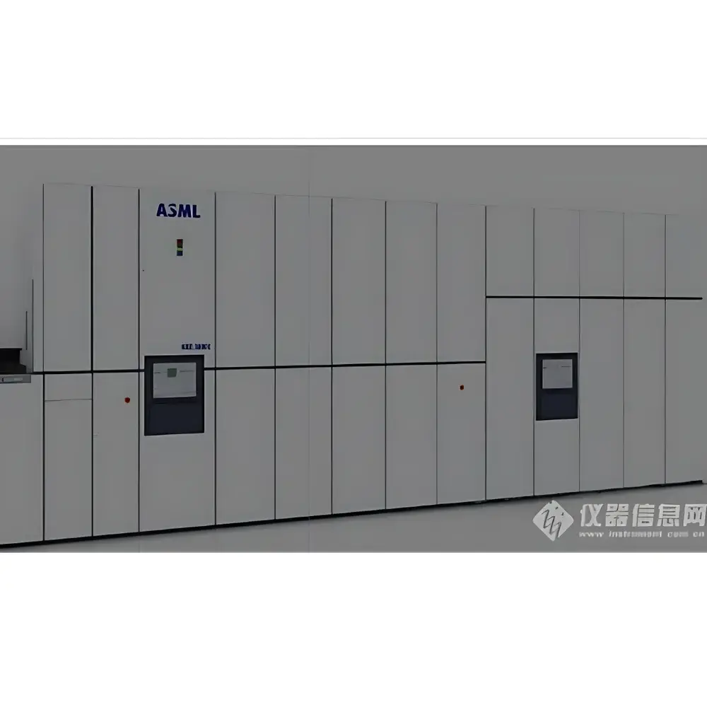
ASML TWINSCAN NXE & NXT Series Lithography Systems for Semiconductor Manufacturing
| Brand | ASML |
|---|---|
| Origin | Netherlands |
| Type | Mask Aligner / Stepper / Scanner |
| Technology | EUV (13.5 nm) and DUV (193 nm ArFi, 248 nm KrF, 365 nm i-line) |
| Numerical Aperture (NA) | 0.75–0.55 |
| Resolution | ≤8 nm (High-NA EUV) to ≤220 nm (i-line) |
| Overlay Accuracy | ≤1.1 nm (NXE:3800E) |
| Throughput | 160–350 wafers/hour (300 mm) |
| Compliance | ISO 14644-1 Class 1 cleanroom integration, SEMI S2/S8 certified, compatible with 21 CFR Part 11 audit trails via integrated metrology interfaces |
Overview
The ASML TWINSCAN NXE and NXT series represent the industry-standard photolithography platforms for advanced semiconductor manufacturing. Engineered for precision pattern transfer onto silicon wafers, these systems operate across multiple exposure wavelengths—enabling process flexibility from legacy packaging and MEMS fabrication to cutting-edge logic and memory nodes. EUV systems (NXE series) utilize synchrotron-generated 13.5 nm radiation in a vacuum environment, coupled with multilayer reflective optics and high-precision wafer and reticle stages. DUV systems (NXT and XT series) employ refractive projection optics with immersion (ArFi) or dry (ArF, KrF, i-line) configurations, supporting both single-exposure and multi-patterning schemes. All platforms integrate real-time interferometric stage positioning, thermal stability control (<±0.01 °C), and adaptive focus/leveling algorithms to maintain sub-nanometer overlay fidelity across full-field exposure.
Key Features
- Modular scanner architecture with field-proven TWINSCAN dual-stage design for continuous exposure and alignment cycles
- High-NA EUV optics (NXE:3800E, NA = 0.55) enabling single-exposure patterning at ≤8 nm half-pitch, with roadmap extension to Hyper-NA (≥0.7) systems under development
- Immersion-enabled ArFi systems (NXT:2050i) delivering ≤38 nm resolution at 193 nm wavelength with NA = 1.35 and <2.5 nm overlay accuracy
- Integrated metrology readiness: native compatibility with ASML YieldStar and HMI eBeam platforms for in-line CD uniformity and overlay error monitoring
- Advanced thermal management system ensuring <50 mK wafer temperature drift over 8-hour operation, critical for overlay stability
- Real-time dose control via laser power stabilization and pulse-to-pulse energy monitoring (±0.3% RMS)
Sample Compatibility & Compliance
These lithography systems support standard 300 mm silicon wafers with front-side alignment marks and backside flat/notch identification. Reticle handling complies with SEMI E127 standards, including pellicle mounting, contamination control (≤0.1 particles >50 nm per cm²/h), and automated defect inspection interfaces. All platforms meet ISO 14644-1 Class 1 cleanroom requirements when installed with ASML-certified air filtration and vibration isolation. From a regulatory standpoint, system-level software architecture supports GLP/GMP-compliant environments through configurable audit trails, electronic signatures, and 21 CFR Part 11–compliant data archiving when paired with ASML’s DeltaTrack or third-party MES integration. Process recipes are traceable to ISO 9001–certified calibration protocols, and optical components undergo annual NA verification per ASTM F2781.
Software & Data Management
Litho systems operate on ASML’s Tachyon platform—a deterministic, real-time control suite managing exposure sequencing, focus mapping, dose optimization, and stage trajectory planning. Tachyon integrates with factory automation via SECS/GEM and OPC UA protocols. Recipe management includes version-controlled parameter sets with hierarchical inheritance (tool → product → layer), enabling rapid ramp-up for new technology nodes. Metrology feedback loops support closed-loop correction of overlay and focus errors using statistical process control (SPC) engines compliant with JMP and Minitab data export formats. Raw exposure logs (including laser pulse history, stage position residuals, and environmental sensor readings) are stored in HDF5 format with SHA-256 checksums for long-term integrity validation.
Applications
- EUV platforms (NXE:3800E/NXE:3600D): High-volume manufacturing of logic ICs at 3 nm and 2 nm nodes; DRAM scaling below 1β; 3D NAND with >200 layers
- ArFi immersion scanners (NXT:2050i/NXT:2000i): Multi-patterning for 7 nm FinFET and GAA transistors; RF-SOI and BCD processes requiring tight CDU
- KrF systems (XT:860N): Analog/mixed-signal ICs, power devices (IGBT, SiC), and MEMS sensors where cost-per-wafer outweighs resolution demands
- i-line scanners (XT:400L): Wafer-level packaging, image sensor BEOL, and discrete device fabrication with relaxed overlay budgets
FAQ
What is the difference between EUV and DUV lithography in terms of process capability?
EUV enables single-exposure patterning below 13 nm half-pitch due to its 13.5 nm wavelength and reflective optics, whereas DUV relies on immersion and multi-patterning to achieve comparable resolution—increasing mask count, cycle time, and defect risk.
Are ASML lithography systems qualified for FDA-regulated medical device manufacturing?
Yes—when deployed with validated Tachyon configurations and documented change control procedures, they support ISO 13485 environments; however, end-user qualification remains the responsibility of the device manufacturer.
How does ASML ensure long-term optical performance stability?
All projection lenses undergo accelerated aging tests per ISO 10110-7, and in-situ wavefront sensing (via reference grating interferometry) enables quarterly NA recalibration without tool downtime.
Can these tools be retrofitted for newer process nodes?
NXT-series platforms support hardware upgrades (e.g., lens exchange, stage enhancement) up to three generations; NXE systems are not field-upgradable beyond firmware and metrology interface updates due to fundamental optical redesign requirements.


