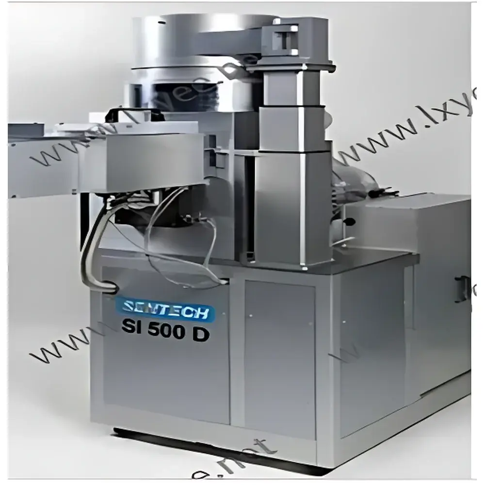

SENTECH SI 500 D Plasma-Enhanced Chemical Vapor Deposition (PECVD) System
| Brand | SENTECH |
|---|---|
| Origin | Germany |
| Model | SI 500 D |
| Plasma Source | Planar Triple-Spiral Antenna (PTSA) |
| Substrate Temperature Range | RT to +350 °C |
| Vacuum System | Fully Integrated, High-Stability |
| Process Compatibility | SiO₂, SiNₓ, SiONₓ, a-Si, SiC, TEOS-derived films |
| Substrate Size | Up to 200 mm wafers or carrier-mounted substrates |
| Optional Features | Load-lock integration, Laser Endpoint Detection, Substrate Biasing, He-backside Cooling with Real-Time Backside Temperature Sensing |
| Control Architecture | SENTECH Fieldbus-Based SCADA Software with Audit-Trail-Capable UI |
| Compliance Context | Designed for GLP/GMP-aligned R&D and pilot-line fabrication |
Overview
The SENTECH SI 500 D is a high-precision, modular plasma-enhanced chemical vapor deposition (PECVD) system engineered for low-damage, low-temperature dielectric and semiconductor thin-film synthesis. It operates on the fundamental principle of inductively coupled, high-density plasma generation via SENTECH’s proprietary Planar Triple-Spiral Antenna (PTSA) source — a planar RF-driven configuration that delivers exceptional plasma uniformity, high electron density (>1 × 10¹¹ cm⁻³), and inherently low ion energy (<10 eV), minimizing substrate bombardment while sustaining robust precursor dissociation. Unlike conventional parallel-plate or ICP reactors, the PTSA architecture enables efficient power coupling at reduced RF forward power (typically 300–800 W), resulting in stable, repeatable film growth under sub-atmospheric pressures (1–100 mTorr). The system is purpose-built for applications demanding atomic-level interface control — including gate dielectrics, passivation layers, encapsulation barriers for organic electronics, and stress-engineered SiNₓ for MEMS packaging — all processed at substrate temperatures ranging from ambient to +350 °C.
Key Features
- Planar Triple-Spiral Antenna (PTSA) plasma source: Enables high plasma density with minimal ion-induced damage and superior radial uniformity across 200 mm substrates.
- Dynamic temperature-controlled substrate electrode: Integrates helium backside cooling, real-time thermocouple-based backside temperature monitoring, and programmable ramp/soak profiles (RT to +350 °C, ±0.5 °C stability).
- Gas delivery architecture with spatially separated precursor inlets: Reduces gas-phase reactions and improves stoichiometric control for multi-component films (e.g., SiONₓ, graded SiNₓ/SiO₂ stacks).
- Fully integrated vacuum system: Includes turbomolecular pumping, capacitance manometer pressure control, and automated vent/pump-down sequences compliant with SEMI S2 safety guidelines.
- SENETCH Fieldbus-based control platform: Provides deterministic I/O response, full recipe management, event logging, and optional 21 CFR Part 11–compliant audit trails with user-role authentication.
- Modular footprint design: Supports standalone operation or integration into SENTECH cluster tools with up to six process modules (PECVD, etch, ALD, sputtering), load-lock transfer, and robotic wafer handling.
Sample Compatibility & Compliance
The SI 500 D accommodates rigid and flexible substrates up to 200 mm in diameter, including silicon wafers, glass, quartz, polymer foils (e.g., PET, PI), and carrier-mounted devices. Its low-temperature capability (<100 °C deposition for many SiO₂ and SiNₓ formulations) makes it suitable for temperature-sensitive organic semiconductors, perovskite precursors, and bio-integrated sensors. The system meets key international standards for cleanroom-compatible equipment: ISO 14644-1 Class 5 airflow compatibility, UL 61010-1 electrical safety certification, and electromagnetic compatibility per EN 61326-1. For regulated environments, the control software supports configurable electronic signatures, change history tracking, and exportable CSV/Excel logs aligned with ISO/IEC 17025 documentation requirements.
Software & Data Management
Operation is managed through SENTECH’s unified GUI — a role-based interface supporting operator, engineer, and administrator access levels. All process parameters (RF power, pressure, gas flows, temperature setpoints, ramp rates) are stored in encrypted recipe files with version timestamps. Real-time data acquisition includes RF forward/reflected power, chamber pressure, substrate temperature (front and back), and optional endpoint signals (e.g., laser interferometry or OES intensity at 427.8 nm for SiNₓ etch/drain monitoring). Raw sensor streams and alarm events are logged with microsecond resolution and can be exported in HDF5 or MATLAB-compatible formats for offline metrology correlation (e.g., ellipsometry, XRR, CV profiling).
Applications
- Low-stress SiNₓ passivation for GaN HEMTs and SiC power devices (breakdown voltage >10 MV/cm, fixed charge density <1 × 10¹¹ cm⁻²).
- Conformal SiO₂ and SiONₓ gate dielectrics for flexible TFT backplanes (mobility retention >95% after 10⁴ bending cycles).
- Hermetic moisture barrier layers on OLED and OPV substrates (WVTR <10⁻⁶ g/m²/day measured by Ca test).
- Amorphous silicon (a-Si) and silicon carbide (SiC) films for photovoltaic antireflection and interlayer applications.
- TEOS-derived oxide films with tunable refractive index (1.44–1.48) and low hydrogen content (<5 at.%) for optical waveguide fabrication.
FAQ
What plasma generation method does the SI 500 D use?
It employs SENTECH’s patented Planar Triple-Spiral Antenna (PTSA), an inductive RF source delivering high-density plasma with low ion energy and excellent radial uniformity.
Can the system deposit films below 100 °C?
Yes — optimized SiO₂ and SiNₓ films are routinely deposited at 25–80 °C, enabling processing of temperature-sensitive organic and 2D materials.
Is load-lock integration available?
Yes — the SI 500 D is compatible with SENTECH’s vacuum load-lock modules for 200 mm wafers, supporting high-throughput batch processing in controlled ambient conditions.
Does the system support endpoint detection?
Laser interferometric endpoint detection is an optional add-on, configurable for real-time monitoring of film thickness during deposition or etch steps.
How is process reproducibility ensured across multiple runs?
Through hardware-level pressure and temperature stabilization, closed-loop RF matching, gas flow calibration traceable to NIST standards, and software-enforced recipe locking with digital signature verification.


