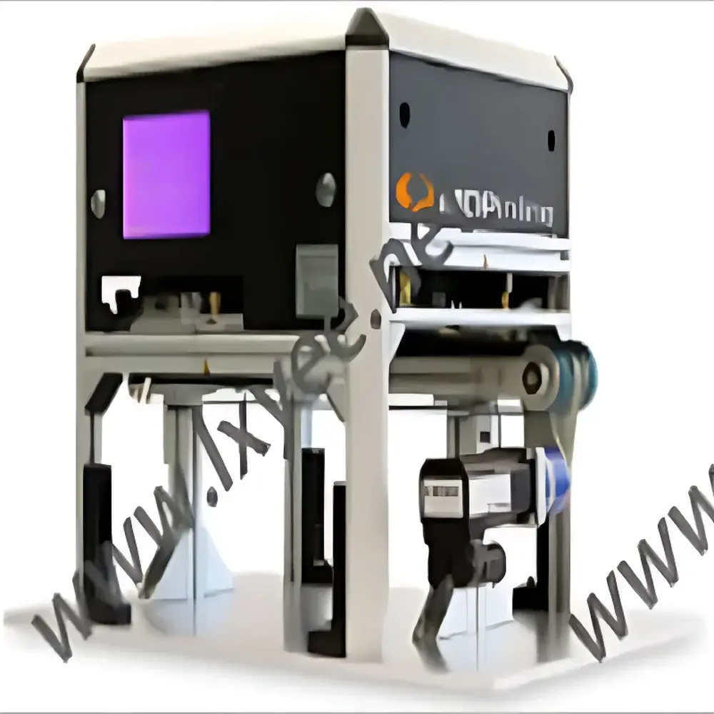

SENTECH MDPinline Inline Minority Carrier Lifetime Tester
| Brand | SENTECH |
|---|---|
| Origin | Germany |
| Model | MDPinline |
| Application | In-line quantitative minority carrier lifetime mapping of silicon wafers |
| Measurement Principle | Microwave-detected photoconductance decay (µ-PCD) |
| Scan Speed | <1 second per wafer |
| Integration | Conveyor-compatible, no moving mechanical parts |
| Compliance | Designed for semiconductor manufacturing environments compliant with ISO 9001 and SEMI S2/S8 safety standards |
| Software Interface | Ethernet-enabled, supports SECS/GEM protocol for factory automation integration |
| Data Output | Full-wafer lifetime map (pixel-resolved), dual-line resistivity profile, CSV/HDF5 export |
| Calibration | Traceable to NIST-traceable reference wafers |
| Operating Environment | Class 1000 cleanroom compatible (ISO 4), 18–28 °C, <60% RH non-condensing |
| Power Supply | 100–240 V AC, 50/60 Hz, <500 W |
Overview
The SENTECH MDPinline is a production-grade, conveyor-integrated minority carrier lifetime tester engineered for real-time, full-wafer characterization in photovoltaic and semiconductor manufacturing lines. It employs microwave-detected photoconductance decay (µ-PCD), a non-contact, non-destructive technique that quantifies bulk recombination kinetics by measuring the transient photoconductance response following laser excitation. Unlike point-probe or scanning-stage systems, the MDPinline operates without mechanical motion—relying instead on synchronized wafer transport and high-speed microwave detection to acquire spatially resolved lifetime maps at sub-second throughput. Its design targets inline deployment at critical process nodes: post-crystal growth, pre-diffusion, post-anneal, and pre-packaging. The system delivers quantitative, pixel-level lifetime data (τeff) across standard 156 mm × 156 mm (M2), 166 mm, 182 mm (M10), and 210 mm (G12) silicon wafers—enabling statistical process control (SPC) at scale.
Key Features
- Sub-second full-wafer mapping: Acquires >10,000 lifetime data points per wafer in <1 s, enabling throughput of >3,600 wafers/hour.
- Motionless architecture: No motors, stages, or optical scanners—eliminates wear, vibration sensitivity, and calibration drift during continuous 24/7 operation.
- Integrated resistivity profiling: Simultaneous dual-line four-point probe resistivity measurement (two orthogonal scans) co-registered with lifetime data.
- Factory automation ready: Native support for SECS/GEM communication protocols; Ethernet/IP interface; compatible with MES and APC systems.
- Robust environmental design: Sealed optical path, ESD-safe housing, and thermal stabilization for stable performance in production-floor conditions (18–28 °C, ISO Class 4 cleanroom).
- Traceable metrology: Calibrated using NIST-traceable reference wafers; lifetime accuracy validated per ASTM F2482–22 (Standard Test Method for Minority Carrier Lifetime of Silicon Wafers).
Sample Compatibility & Compliance
The MDPinline is optimized for monocrystalline and multicrystalline Czochralski (CZ) and float-zone (FZ) silicon wafers ranging from 100 µm to 300 µm thickness. It accommodates standard PV wafer formats (M2–G12) and handles both textured and planar surfaces without adjustment. The system complies with SEMI S2 (safety) and S8 (ergonomics) standards, and its electrical design meets IEC 61000-6-2/6-4 for industrial electromagnetic compatibility. Data integrity adheres to principles aligned with FDA 21 CFR Part 11 requirements—including electronic audit trails, user access controls, and immutable raw-data archiving—when deployed with SENTECH’s optional IQ/OQ validation package and compliant LIMS integration.
Software & Data Management
Control and analysis are performed via SENTECH’s MDP Control Suite v4.x—a Windows-based application supporting real-time visualization, SPC charting (X-bar/R, Cpk), and automated defect clustering (e.g., grain boundary segregation, dislocation clusters, oxygen precipitate zones). All raw microwave decay waveforms, lifetime maps, and resistivity profiles are stored in HDF5 format for traceability and third-party analysis (Python/Matlab). The software includes configurable pass/fail thresholds, batch reporting (PDF/Excel), and direct export to JMP, Spotfire, or FactoryTalk Analytics. Optional modules enable predictive maintenance alerts based on signal-to-noise ratio (SNR) degradation and lifetime map entropy trending.
Applications
- Crystal growth monitoring: Statistical evaluation of >10,000 wafers over 3 hours reveals furnace temperature gradient anomalies and dopant segregation patterns.
- Diffusion process control: Quantifies lateral uniformity of emitter saturation current density (J0e) via lifetime correlation with sheet resistance.
- Surface passivation validation: Measures local τeff improvement after SiNx:H, Al2O3, or TOPCon layer deposition—identifying edge recombination or pinhole defects.
- Material sorting: Enables binning by lifetime quartiles prior to cell fabrication, improving final module power yield variance by up to 15% (field-validated).
- Root cause analysis: Correlates localized lifetime minima with X-ray diffraction (XRD) or photoluminescence (PL) data to isolate metal contamination or dislocation density gradients.
FAQ
What measurement principle does the MDPinline use?
It uses microwave-detected photoconductance decay (µ-PCD), where a pulsed laser generates excess carriers, and their recombination-induced change in microwave reflectance is measured to calculate effective minority carrier lifetime.
Can it measure wafers with anti-reflective coatings or texturing?
Yes—the 1.06 µm Nd:YAG laser and optimized microwave coupling accommodate standard SiNx:H ARC and random pyramids without signal loss or recalibration.
Is resistivity measurement quantitative or qualitative?
Quantitative: Dual-line four-point probe scan yields absolute sheet resistance values (Ω/sq) with ±3% repeatability, traceable to PTB-certified standards.
How is system validation performed for GMP environments?
SENTECH provides IQ/OQ documentation packages, including installation verification, operational range testing, linearity assessment per ASTM F2482, and electronic record integrity checks per 21 CFR Part 11 Annex 11 guidelines.
Does it require periodic recalibration?
No routine recalibration is needed; however, annual performance verification using certified reference wafers is recommended to maintain metrological traceability.


