Siegert Wafer Borofloat® and Fused Silica Glass Wafers
| Brand | Siegert Wafer |
|---|---|
| Origin | Germany |
| Model | Siegert Wafer Series |
| Material Options | Borofloat® 33, Fused Silica |
| Diameter | Up to 200 mm |
| Thickness | 0.5–2.0 mm |
| Shape | Round or Rectangular |
| Surface Coatings | ITO, Photoresist, Custom Thin-Film Layers |
| Compliance | ISO 14644-1 Class 5 Cleanroom Processing |
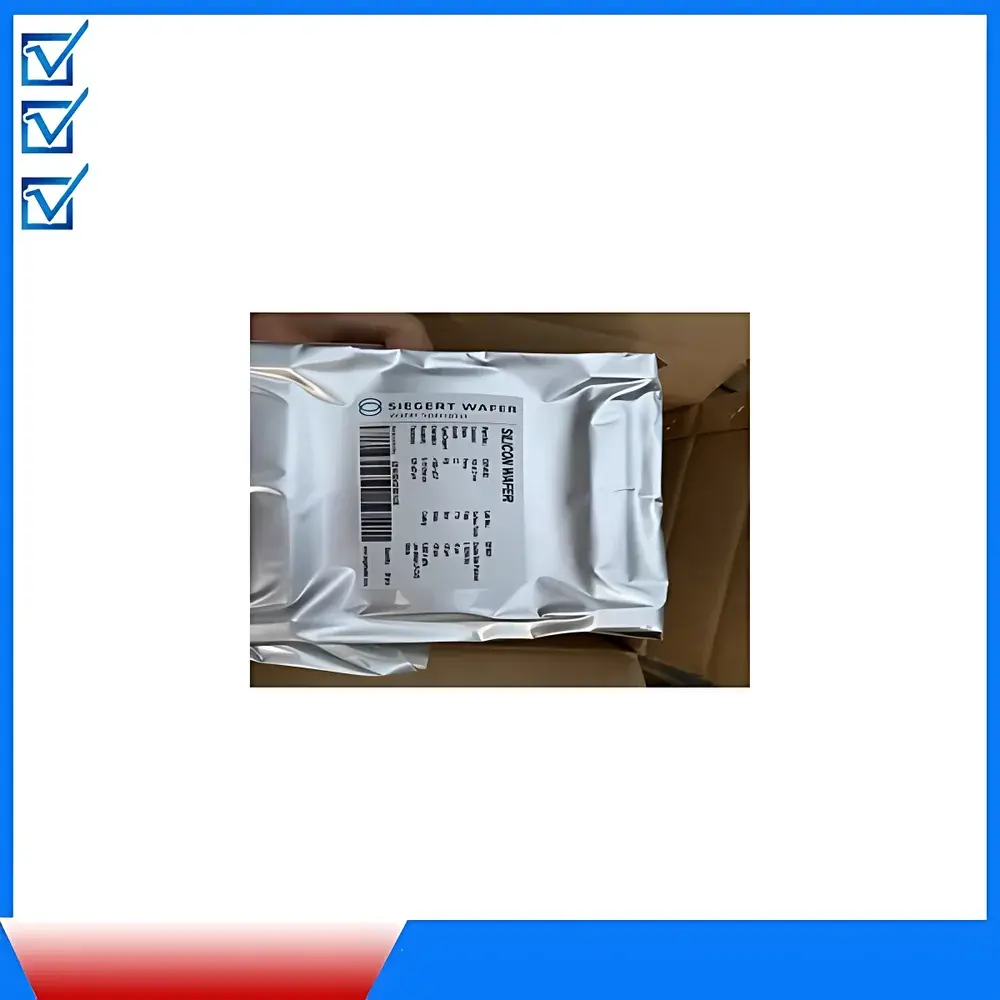
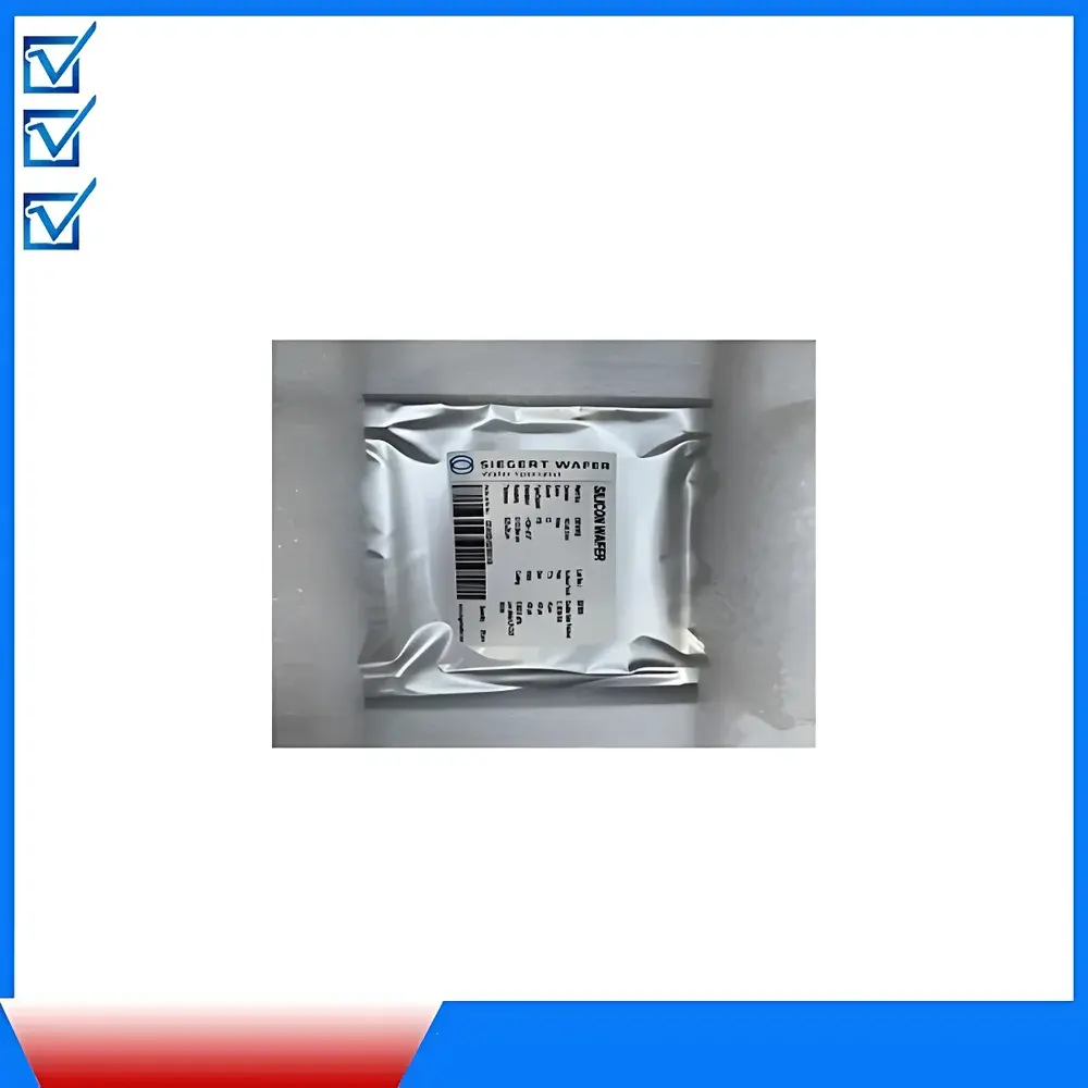
| Packaging | Vacuum-Sealed, Particle-Free Cassette |
Overview
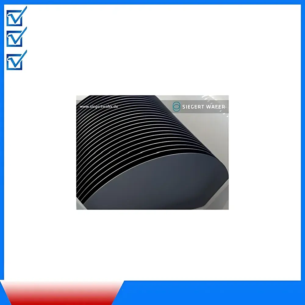
Siegert Wafer glass wafers are precision-engineered substrates manufactured in Germany for high-stability applications in semiconductor R&D, micro-optics, MEMS packaging, and advanced sensor development. Unlike silicon wafers, these optical-grade glass wafers leverage the exceptional thermal, mechanical, and optical homogeneity of Borofloat® 33 (a borosilicate glass) and fused silica—materials selected for their near-zero thermal expansion coefficients, high transmission across UV–VIS–NIR spectra, and resistance to chemical etching and thermal shock. The wafers are produced under controlled cleanroom conditions (ISO 14644-1 Class 5), with surface flatness maintained within λ/10 (at 633 nm) and total thickness variation (TTV) < 1 µm over full diameter. Their non-conductive nature, combined with tunable surface functionalization, makes them ideal for applications where electrical isolation, optical transparency, or hermetic sealing is critical—such as cap wafers in cavity packaging, carrier substrates for thin-film deposition, or master substrates for nanoimprint lithography.
Key Features
- Precision ground and polished surfaces with RMS roughness < 0.3 nm (measured by AFM), enabling direct bonding and high-fidelity thin-film adhesion.
- Material traceability per batch, including certified thermal expansion coefficient (α = 3.25 × 10⁻⁶ K⁻¹ for Borofloat® 33; α = 0.55 × 10⁻⁶ K⁻¹ for fused silica) and refractive index data (n = 1.472 @ 589 nm).
- Standard and custom geometries: round wafers up to Ø200 mm, rectangular blanks up to 150 × 150 mm, with edge profiles optimized for handling in automated wafer probers and aligners.
- Optional surface modifications: sputtered ITO layers (sheet resistance 10–100 Ω/sq, >85% transmittance @ 550 nm), spin-coated photoresist (e.g., AZ® 1518 or LOR® 3A), and anti-reflective or hydrophobic dielectric coatings.
- Controlled annealing cycles post-polishing to eliminate residual stress and ensure long-term dimensional stability under thermal cycling (−40 °C to +300 °C).
Sample Compatibility & Compliance
Siegert Wafer substrates are compatible with standard semiconductor fabrication toolsets—including PECVD, e-beam evaporation, reactive ion etching (RIE), and wafer-level bonding systems (anodic, fusion, and adhesive). All wafers undergo rigorous particle inspection (per SEMI F20) and surface metal contamination screening (ICP-MS for Na, K, Fe, Cr, Ni ≤ 1 × 10¹⁰ atoms/cm²). Documentation includes Certificate of Conformance (CoC) with material lot ID, dimensional verification report (CMM-measured), and spectral transmittance curves. Products comply with SEMI standards for substrate cleanliness (SEMI F19, F57), and are suitable for use in GLP- and GMP-regulated environments when paired with appropriate process validation protocols.
Software & Data Management
While Siegert Wafer substrates are passive components, they integrate seamlessly into traceability workflows supported by industry-standard MES platforms (e.g., Applied Materials Envision, Brooks Automation AutoTrack). Each wafer shipment includes a QR-coded label linking to a secure digital dossier containing metrology reports, coating thickness maps (via ellipsometry), and environmental exposure logs. For customers operating under FDA 21 CFR Part 11 requirements, Siegert provides audit-ready documentation packages—including electronic signatures on CoCs and revision-controlled release notes for all coating process changes.
Applications
- Semiconductor: Capping wafers for MEMS inertial sensors and pressure die; carrier substrates for GaN-on-glass epitaxy and flexible hybrid electronics.
- Optics & Photonics: Substrates for diffractive optical elements (DOEs), micro-lens arrays, and integrated waveguide platforms requiring low birefringence and high UV transmission.
- Microfluidics & Lab-on-Chip: Chemically resistant base wafers for glass-PDMS bonding, with pre-patterned ITO electrodes enabling electrokinetic actuation.
- Research & Development: Calibration standards for profilometry and interferometry; reference substrates in EUV lithography mask blank qualification.
- Advanced Packaging: Interposer wafers for 2.5D/3D heterogeneous integration, leveraging glass’s CTE match with Si and Cu redistribution layers.
FAQ
Are Siegert Wafer glass substrates available with backside metallization?
Yes—custom Ti/Pt/Au or Cr/Au stacks can be deposited via e-beam evaporation upon request, with thickness control ±2 nm and adhesion validated per ASTM B571.
What is the maximum usable temperature for Borofloat® 33 wafers during processing?
Continuous use up to 450 °C is permissible; short-term excursions to 500 °C are allowable with controlled ramp rates (< 5 °C/min) to avoid thermal fracture.
Can rectangular glass wafers be supplied with alignment flats or notches?
Yes—standard alignment features (e.g., single flat, dual notch per SEMI M1) are available on rectangular blanks up to 125 × 125 mm, with positional tolerance ±0.1 mm.
Do you provide wafer-level metrology data for each shipment?
Every order includes full metrology: TTV, bow, warp, surface roughness (AFM), and coating uniformity (ellipsometry at ≥9 points across diameter).
Is there lead time reduction for standard-dimension wafers?
Yes—Ø100 mm and Ø150 mm Borofloat® 33 wafers (0.7 mm and 1.0 mm thick) are held in EU-based inventory, enabling shipment within 5 business days of order confirmation.


