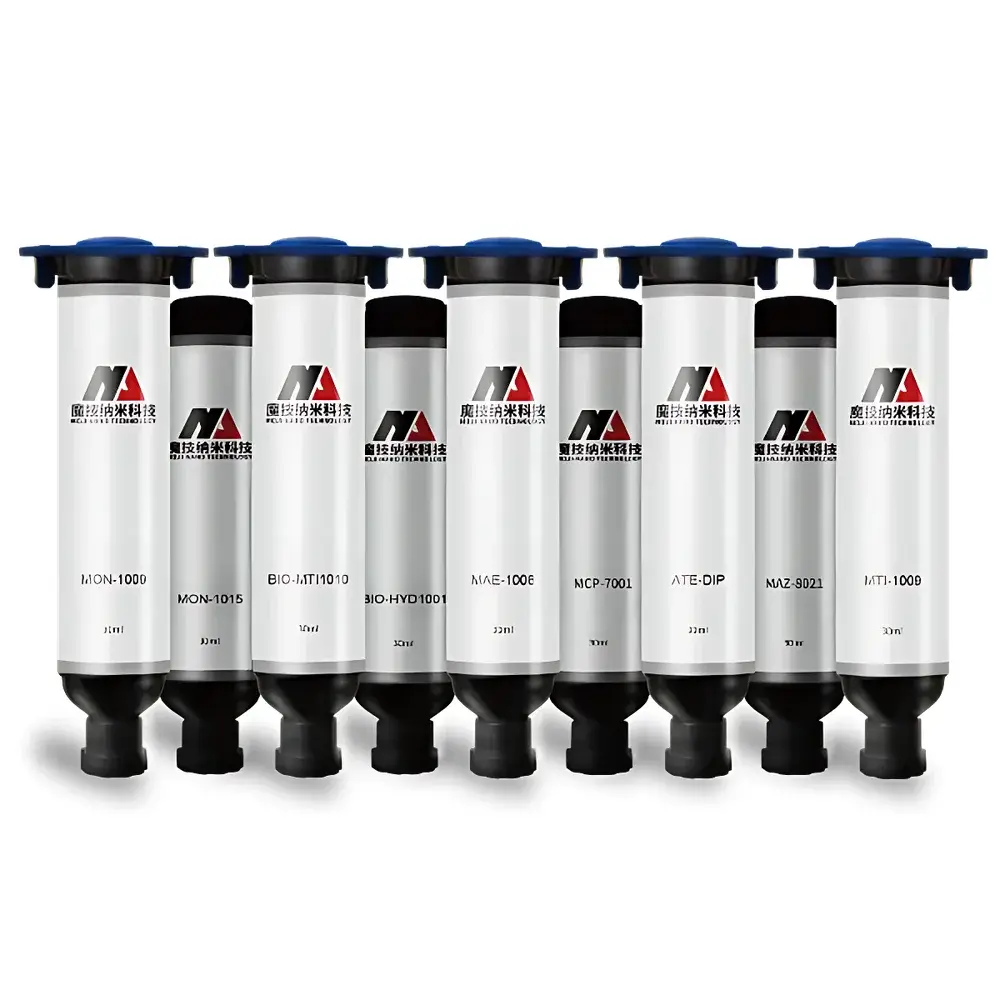
MOJI-NANO 3D Micro/Nano-Scale Photoresist for Multiphoton Lithography
| Brand | MOJI-NANO |
|---|---|
| Origin | Shandong, China |
| Manufacturer Type | Original Equipment Manufacturer (OEM) & Material Developer |
| Product Category | Domestic Advanced Photoresist for Maskless Direct Laser Writing |
| Model | 3D Micro/Nano-Scale Photoresist Series |
| Pricing | Available upon Technical Consultation |
Overview
MOJI-NANO 3D Micro/Nano-Scale Photoresist is a proprietary class of high-performance photochemically active resins engineered for multiphoton absorption lithography (MPAL) using near-infrared (NIR) or visible femtosecond pulsed lasers. Unlike conventional UV-based photolithography resists, this material system leverages nonlinear optical excitation—where two or more photons are simultaneously absorbed within a tightly focused laser volume—to achieve true three-dimensional voxel-by-voxel polymerization. This enables sub-diffraction-limit spatial confinement, supporting feature resolution down to ≤70 nm in optimized process conditions. The resist formulation exhibits high transparency across 700–1050 nm wavelengths, low nonspecific background polymerization, and robust post-processing stability during development, critical for fabricating freestanding micro-optical elements, hierarchical microfluidic networks, and metamaterial unit cells with high aspect ratios and mechanical integrity.
Key Features
- Engineered for multiphoton polymerization (MPP) with femtosecond laser sources (e.g., Ti:sapphire, Yb-fiber, or frequency-doubled systems)
- Nanometer-scale line width control (≤70 nm demonstrated under calibrated direct laser writing)
- High optical transmittance (>90% at 780 nm), minimizing scattering-induced voxel distortion
- Controlled solubility contrast between exposed/unexposed regions, enabling high-fidelity development in standard organic solvents (e.g., PGMEA, IPA)
- Excellent thermal and oxidative stability—retains structural fidelity up to 200 °C in inert atmosphere
- Tailored mechanical properties: Young’s modulus tunable from 0.5 GPa to >3 GPa via crosslink density modulation
- Batch-to-batch reproducibility validated per ISO 9001-certified manufacturing protocols
Sample Compatibility & Compliance
The photoresist demonstrates broad compatibility with fused silica, silicon wafers, ITO-coated glass, and flexible polymer substrates (e.g., PET, PI). It supports both spin-coating (thickness range: 100 nm – 5 µm) and drop-cast deposition, with uniform film formation verified by ellipsometry and AFM surface roughness analysis (Rq < 0.8 nm over 10 × 10 µm²). All formulations comply with RoHS Directive 2011/65/EU and are free of halogenated solvents and heavy-metal catalysts. For regulated applications—including biomedical microdevices and photonics integrated circuits—the resist series is compatible with cleanroom Class 100 (ISO 5) processing environments and meets baseline requirements for GLP-compliant fabrication workflows. Documentation packages include full SDS, lot-specific QC reports, and traceability records aligned with ISO/IEC 17025 guidelines.
Software & Data Management
While the photoresist itself is a consumable material, its integration into automated nanofabrication platforms is supported through standardized process parameter libraries for leading commercial MPP systems (e.g., Nanoscribe Quantum X, UpNano NanoOne, and custom-built laser scanning stages). MOJI-NANO provides detailed exposure dose calibration curves (J/cm² vs. linewidth/height), developer concentration/time matrices, and post-bake optimization profiles. All technical documentation is delivered in English with metadata compliant with ASTM E2500-21 (Standard Guide for Specification, Design, and Verification of Pharmaceutical and Biopharmaceutical Manufacturing Systems and Equipment), facilitating audit readiness for FDA 21 CFR Part 11–governed environments where electronic records and signatures apply.
Applications
- Freeform micro-optics: graded-index lenses, beam shapers, and polarization-selective waveguides
- Microfluidic architectures: monolithic 3D channels, valves, mixers, and organ-on-chip scaffolds
- Metamaterials and photonic crystals: lattice structures with sub-wavelength periodicity and negative refractive index behavior
- Biosensing interfaces: high-surface-area 3D hydrogel scaffolds functionalized with antibodies or aptamers
- MEMS packaging: hermetic encapsulation layers and stress-engineered release membranes
- Quantum device prototyping: solid-state spin qubit hosts and nanophotonic cavity arrays
FAQ
What laser wavelengths are compatible with this photoresist?
The resist is optimized for femtosecond pulsed lasers operating at 780 nm, 800 nm, and 1040 nm; visible-range compatibility (e.g., 515 nm) is achievable with appropriate sensitizer doping—consult technical datasheet for wavelength-specific quantum yield data.
Is the material compatible with electron-beam lithography (EBL)?
No—this formulation is specifically designed for nonlinear optical excitation and lacks the electron-scattering cross-section required for high-resolution EBL. It is not recommended as an e-beam resist.
Can the resist be used for grayscale lithography?
Yes—dose-controlled multiphoton exposure enables continuous-tone 3D structuring, making it suitable for diffractive optical element (DOE) fabrication and topography-mapped microstructures.
What is the shelf life and storage requirement?
Unopened vials retain performance for ≥12 months when stored at 4 °C in nitrogen-purged, light-blocking containers. Prior to use, equilibrate to room temperature for ≥2 hours to prevent condensation.
Do you provide process development support?
Yes—MOJI-NANO offers application engineering services including resist selection guidance, exposure parameter optimization, and integration assistance with third-party lithography platforms under NDA.
Related Products


