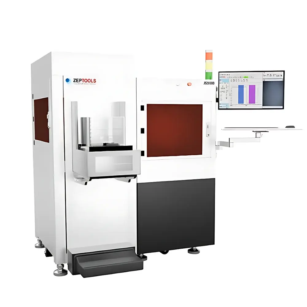
ZEPTOOLS JS2000C Automated Stylus Profilometer
| Brand | ZEPTOOLS |
|---|---|
| Model | JS2000C |
| Measurement Principle | Inductive |
| Vertical Measurement Range | 10 nm – 80 µm |
| Probe Tip Radius | 1 µm / 2 µm |
| Normal Force Range | 0.5–50 mg |
| Scan Length | ≤50 mm |
| Step Height Repeatability | <0.5 nm |
| Vertical Resolution | 0.05 nm |
| Wafer Compatibility | 150 mm (6″) and 200 mm (8″) |
| Maximum Wafer Thickness | 50 mm |
| Positioning Accuracy (Vision System) | ±10 µm |
| Mechanical Stability | >500 consecutive wafers in marathon testing |
| Throughput | ≥10 WPH (single-side, ≥5 measurement positions) |
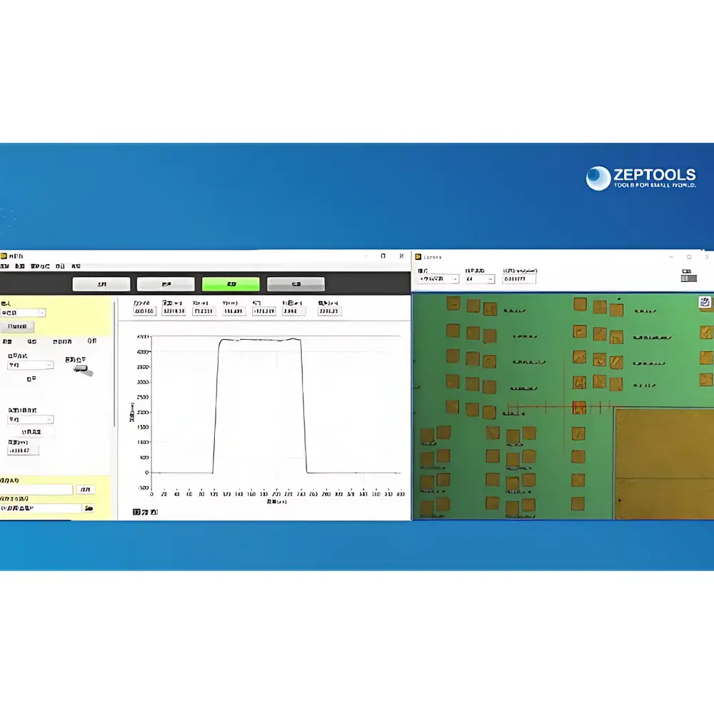
Overview
The ZEPTOOLS JS2000C is an automated stylus profilometer engineered for high-precision, traceable step height and surface topography characterization in advanced semiconductor fabrication, thin-film R&D, and precision materials laboratories. It operates on the principle of inductive displacement sensing, where a mechanically scanned diamond-tipped probe traverses the sample surface, converting minute vertical deflections into high-fidelity analog signals via a linear variable differential transformer (LVDT)-based transducer. This architecture delivers sub-nanometer vertical resolution and exceptional long-term stability—critical for quantifying film thickness variations, etch depth uniformity, CMP endpoint verification, and stress-induced wafer bow. The instrument’s monolithic granite base minimizes thermal drift and vibration coupling, while its integrated dual-color imaging system enables real-time, distortion-free visualization of both probe tip engagement and feature geometry—ensuring accurate placement over sub-micron alignment marks or patterned structures.
Key Features
- Monolithic granite frame with active vibration isolation design for metrological-grade mechanical stability
- Dual high-resolution color cameras (coaxial + oblique) supporting simultaneous tip–sample observation and sub-10 µm visual positioning accuracy
- Programmable probe normal force control (0.5–50 mg) optimized for fragile films, low-k dielectrics, and soft polymer layers
- Automated multi-point scanning routines with customizable grid patterns, looped sequences, and conditional logic for unattended batch operation
- Modular stage architecture accommodating 150 mm and 200 mm wafers; configurable chuck vacuum ports and edge-sensing for repeatable loading
- Real-time signal conditioning with adaptive filtering and digital noise suppression to preserve true surface morphology at 0.05 nm vertical resolution
Sample Compatibility & Compliance
The JS2000C supports rigid and semi-rigid substrates including silicon, sapphire, fused silica, and compound semiconductor wafers up to 50 mm thick. Its low-force probing capability ensures non-destructive profiling of ultra-thin ALD films (<5 nm), photoresists, spin-on glass, and MEMS cantilevers. The system conforms to ISO 25178-2 (areal surface texture parameters), ISO 5436-1 (profile measurement standards), and ASTM E1399 (standard practice for measuring step height using contact profilometry). All measurement data include embedded metadata (timestamp, operator ID, calibration certificate ID, environmental conditions) to support GLP/GMP audit trails and FDA 21 CFR Part 11-compliant electronic records when integrated with validated LIMS environments.
Software & Data Management
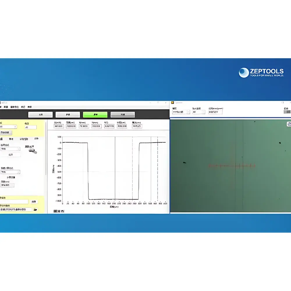
ZEPTOOLS ProfilSoft v4.x provides a deterministic, scriptable platform for acquisition, analysis, and reporting. Core modules include cross-sectional profile extraction, 3D surface reconstruction, film thickness calculation (via step-edge integration), roughness parameter computation (Ra, Rq, Rz, Sk, Spk per ISO 4287/ISO 25178), and curvature-derived stress mapping. Batch processing workflows support automated report generation in PDF/XLSX formats with configurable templates compliant with internal QA checklists or customer-specific DMR requirements. Raw data are stored in HDF5 format with lossless compression and full metadata embedding—enabling reproducible reanalysis and third-party interoperability (e.g., MATLAB, Python via h5py).
Applications
- Quantitative thickness metrology of deposited or etched layers in front-end-of-line (FEOL) and back-end-of-line (BEOL) processes
- Surface roughness and waviness assessment of polished wafers, epitaxial layers, and SOI substrates
- Warpage and global flatness evaluation of bonded wafers and TSV-processed stacks
- Stress calculation from curvature measurements using Stoney’s equation with temperature-compensated reference baselines
- 3D topographic mapping of microfluidic channels, diffractive optical elements, and nanoimprint lithography masters
- Process window qualification for dry/wet etch, PVD/CVD, and electroplating steps across production lots
FAQ
What is the maximum measurable step height on the JS2000C?
The instrument achieves a vertical range of up to 80 µm in standard configuration; extended-range modes (up to 160 µm) are available via optional sensor calibration and software licensing.
Can the JS2000C measure on patterned wafers with sub-micron features?
Yes—the 1 µm radius probe tip, combined with vision-guided positioning and real-time force feedback, enables reliable tracing across dense line/space arrays down to 300 nm pitch without tip snagging or signal dropout.
Is the system compatible with cleanroom Class 100 environments?
The JS2000C meets SEMI S2-0201 safety guidelines and can be configured with HEPA-filtered purge air connections and static-dissipative enclosures for ISO Class 5 (Class 100) integration.
How is traceability maintained for calibration and measurement uncertainty?
Each unit ships with NIST-traceable step height artifacts (SiO₂-on-Si, Cr-on-glass), a full uncertainty budget per ISO/IEC 17025, and annual recalibration services aligned with national metrology institutes.
Does the software support automated pass/fail decision logic for inline process control?
Yes—ProfilSoft includes configurable tolerance zones, statistical process control (SPC) charting, and OPC UA interface for direct integration into factory MES systems.