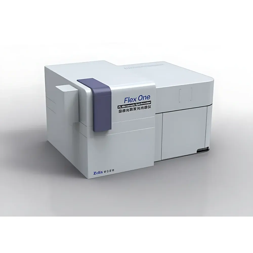
ZOLIX Flex One Micro-Photoluminescence Spectrometer
| Brand | ZOLIX |
|---|---|
| Origin | Beijing, China |
| Manufacturer Type | Original Equipment Manufacturer (OEM) |
| Product Category | Domestic |
| Model | Flex One |
| Instrument Architecture | Dual-Wavelength Excitation Pathway |
| Detector Type | Scientific-grade Cooled CCD |
| Spectral Range | 300–2200 nm |
| Wavelength Accuracy | ±0.2 nm |
| Spectral Resolution | 0.1 nm (typical, configuration-dependent) |
| Spectral Bandwidth | 0.05 nm |
| Stray Light Level | <1×10⁻⁵ |
| Automation Level | Motorized Wavelength Scanning & Positioning |
| Optional Modules | Automated Mapping (50 mm × 50 mm stage), Electroluminescence (EL) Integration, Micro-Raman Coupling, Cryogenic Sample Stage (<10 K) |
Overview
The ZOLIX Flex One Micro-Photoluminescence Spectrometer is an integrated, research-grade optical characterization platform engineered for high-sensitivity, spatially resolved photoluminescence (PL) spectroscopy across the ultraviolet to short-wave infrared spectrum (300–2200 nm). Unlike conventional microscope-coupled PL systems that rely on off-the-shelf optical components, the Flex One employs a purpose-built, alignment-optimized optical architecture grounded in over a decade of ZOLIX’s expertise in fluorescence spectroscopy and spectral system integration. Its core measurement principle is based on resonant or bandgap-excited luminescence: incident photons—delivered via selectable laser sources (e.g., 325 nm, 532 nm, 785 nm)—induce electron-hole pair generation in semiconducting or luminescent materials; the resulting radiative recombination is dispersed by a high-fidelity Czerny-Turner spectrometer and detected with thermoelectrically cooled scientific CCD or InGaAs array detectors. This enables quantitative analysis of critical optoelectronic parameters—including bandgap energy, defect-related emission (e.g., yellow luminescence in GaN), quantum well confinement effects, carrier lifetime proxies, and compositional homogeneity—without physical contact or sample destruction.
Key Features
- Monolithic optical alignment architecture: All critical optical elements—including excitation path routing, collection optics, and spectrometer input slit—are factory-aligned and mechanically stabilized. Re-alignment is required only during initial installation, ensuring long-term repeatability and minimizing user intervention.
- Dual-axis illumination flexibility: Independent horizontal and vertical excitation pathways allow seamless switching between top-down and side-illumination configurations—essential for opaque substrates, packaged devices, or cryostat-integrated measurements.
- Extended spectral coverage: Standard configuration supports 300–2200 nm detection using interchangeable detector modules (CCD: 300–1000 nm; extended-range InGaAs: 800–1700 nm or 800–2200 nm), enabling comprehensive analysis of wide-bandgap nitrides (e.g., AlGaN), mid-gap chalcogenides (e.g., MoS₂), and low-bandgap antimonides (e.g., InSb).
- Real-time video-guided micro-positioning: Integrated CMOS camera provides diffraction-limited visual feedback synchronized with the excitation and collection axes, facilitating sub-100 µm spot targeting on heterogeneous or patterned samples.
- Factory-calibrated spectral response correction: Built-in emission spectrum normalization compensates for wavelength-dependent detector quantum efficiency and grating blaze function, yielding intensity-accurate, inter-laboratory comparable spectra compliant with ASTM E275 and ISO 17025 traceability frameworks.
- Modular expansion capability: Optional hardware add-ons include motorized XYZ mapping stages (50 mm × 50 mm travel, 1 µm repeatability), electroluminescence biasing units (±100 V, 100 mA), Raman spectrometer coupling kits (with notch/edge filters), and vacuum-compatible cryogenic sample holders (base temperature <10 K, compatible with closed-cycle He refrigerators).
Sample Compatibility & Compliance
The Flex One accommodates diverse solid-state specimens—including bulk crystals, epitaxial wafers (SiC, sapphire, Si), thin-film heterostructures (InGaN/GaN MQWs), 2D materials (graphene, TMDs), perovskite films, and optoelectronic devices (LED chips, laser diodes, photodetectors). Its open optical design permits direct integration with commercial cryostats (e.g., Janis ST-500, Montana Instruments Cryostation), magnetic field probes (up to 9 T), and electrochemical cells. All firmware and data acquisition routines adhere to GLP/GMP-relevant audit trail requirements: full metadata logging (timestamp, excitation power, integration time, detector temperature, stage coordinates), electronic signature support, and optional 21 CFR Part 11 compliance packages for regulated environments.
Software & Data Management
Control and analysis are performed via ZOLIX SpectraMaster™ v4.x—a Windows-based application developed in accordance with IEC 62443 cybersecurity guidelines. The software features real-time spectral preview, multi-channel synchronous acquisition (PL + EL + Raman), batch processing with Python API hooks, and automated peak fitting using Voigt or Gaussian deconvolution models. Raw data is saved in HDF5 format (ISO/IEC 15890 compliant), preserving hierarchical metadata, instrument calibration records, and user annotations. Export options include ASCII, CSV, and JCAMP-DX for interoperability with OriginLab, MATLAB, and Thermo Fisher OMNIC platforms.
Applications
- Band structure characterization of III–V and II–VI semiconductors (e.g., GaN, ZnO, CdSe) via temperature-dependent PL mapping.
- Quantum dot size distribution analysis through excitonic peak broadening and Stokes shift quantification.
- Defect spectroscopy in wide-bandgap materials—identifying deep-level traps via low-temperature PL quenching behavior.
- Process monitoring of MOCVD/MBE-grown heterostructures, including interfacial strain assessment via phonon-assisted PL sidebands.
- Failure analysis of micro-LED arrays using spatially resolved EL-PL correlation mapping.
- Low-dimensional material screening (e.g., monolayer WS₂ PL quantum yield vs. dielectric environment).
FAQ
What laser wavelengths are supported natively, and can custom lasers be integrated?
Standard configurations include 325 nm (HeCd), 405 nm (diode), 442 nm (HeCd), 473 nm (DPSS), 532 nm (DPSS), 633 nm (HeNe), and 785 nm (diode). External laser ports accept free-space beams up to 8 mm diameter and support OEM integration of tunable OPOs or ultrafast Ti:sapphire systems.
Is spectral calibration traceable to NIST standards?
Yes—each system ships with a certified Hg/Ar/Ne emission lamp calibration kit. Wavelength accuracy (±0.2 nm) and resolution (0.1 nm) are verified against NIST-traceable line sources and documented in the Certificate of Conformance.
Can the Flex One perform time-resolved PL measurements?
Time-resolved capability requires optional TCSPC module (PicoHarp 300 or HydraHarp 400) and pulsed laser synchronization. This configuration is available as a factory-integrated option with full software co-registration.
What is the minimum detectable PL signal under standard conditions?
With 30 mW 325 nm excitation and 1 s integration on a cooled CCD (−60°C), the system achieves a signal-to-noise ratio >1000:1 for GaN near-band-edge emission, corresponding to ~10⁴ photons/s at the detector plane.
Does the system support automated report generation for QA/QC workflows?
Yes—SpectraMaster includes configurable report templates (PDF/DOCX) with embedded pass/fail criteria, statistical process control (SPC) charts, and digital signature fields aligned with ISO 17025 clause 7.8.2.