Chotest SuperViewW Series Ultra-Smooth Silicon Wafer Surface Optical Profilometer
| Brand | Chotest |
|---|---|
| Origin | Guangdong, China |
| Manufacturer Type | Authorized Distributor |
| Country of Origin | China |
| Model | W412 |
| Price | USD 135,000 (FOB Guangdong) |
Overview
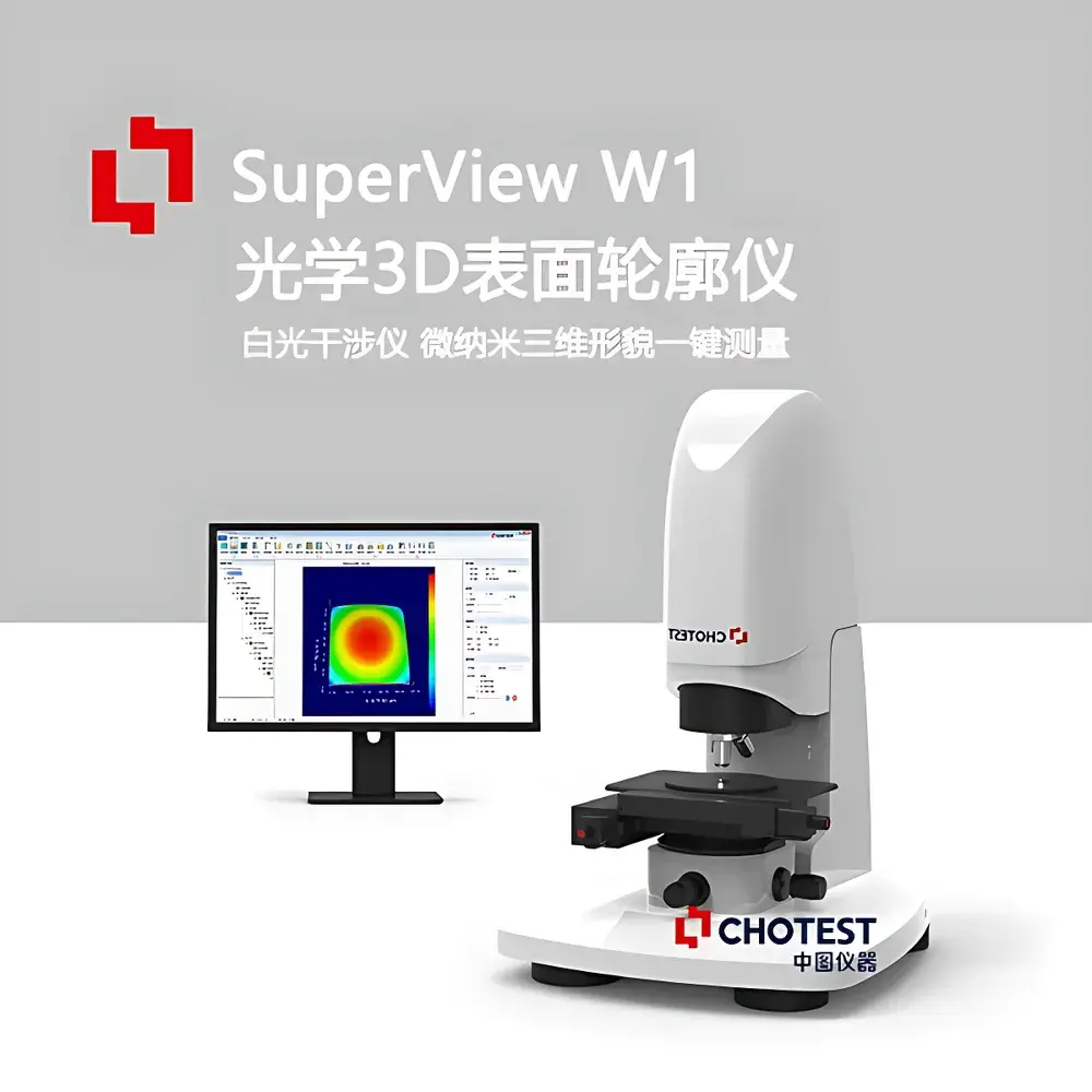
The Chotest SuperViewW Series Ultra-Smooth Silicon Wafer Surface Optical Profilometer is a high-precision, non-contact 3D surface metrology system engineered for nanoscale topographic characterization of semiconductor wafers, optical components, and precision-engineered surfaces. Based on white-light interferometry (WLI), the system delivers sub-nanometer vertical resolution and exceptional measurement repeatability under real-world industrial conditions. Its core architecture integrates a vibration-isolated air-bearing stage, environmental noise compensation algorithms, and a thermally stable optical path—enabling reliable quantification of surface roughness (Rq, Ra, Rsk, etc.), step height, curvature, flatness, and micro-geometric form across diverse material classes—from highly reflective silicon and fused silica to low-reflectivity metals, black anodized alloys, and transparent polymer films.
Key Features
- Sub-nanometer vertical resolution (0.1 nm) with RMS repeatability ≤ 0.005 nm for surface roughness measurements
- White-light interferometry engine with calibrated accuracy of ±0.3% for step-height metrology (e.g., 916.5 nm reference steps)
- Z-axis scanning range up to 10 mm, supporting both single-scan and automated multi-field stitching (square, circular, grid-based)
- High-speed acquisition at 8 µm/s lateral scan velocity while maintaining 0.1 nm vertical resolution
- Modular objective turret accommodating 2.5×, 5×, 10×, 20×, 50×, and 100× interference objectives (standard 10× included)
- 320 × 200 mm motorized XY stage with programmable positioning and auto-focus capability
- Integrated environmental monitoring (temperature, humidity, acoustic noise) for traceable measurement uncertainty assessment per ISO/IEC 17025 guidelines
Sample Compatibility & Compliance
The SuperViewW W412 is validated for measurement of surfaces spanning >6 orders of magnitude in roughness (0.01 nm to >10 µm Rq) and reflectivity (0.1% to >99%). It accommodates substrates ranging from 2-inch to 300-mm silicon wafers, molded glass displays, MEMS cantilevers, injection-molded plastic optics, and coated automotive bearing surfaces. All measurement algorithms comply with ISO 25178-2 (areal surface texture), ISO 4287 (profile-based roughness), ASME B46.1, and SEMI MF1529 (semiconductor wafer surface inspection). The system supports audit-ready data integrity via configurable user roles, electronic signatures, and full measurement history logging aligned with FDA 21 CFR Part 11 requirements for regulated environments.
Software & Data Management
XtremeVision Pro v2.0—the proprietary 3D analysis platform—provides native support for both white-light interferometry and confocal modes within a unified interface. It automatically detects instrument model (W/VT/WT series), calibrates sensor response in real time, and enables direct extraction of geometric parameters including slope angles, radius of curvature, volume, area, and peak-valley distances without post-processing scripting. Batch analysis workflows allow parallel processing of hundreds of fields-of-view; results export natively to Excel (.xlsx), Word (.docx), PDF, CSV, and industry-standard STP/IGES formats. All raw interferograms and metadata are stored in vendor-neutral HDF5 containers, ensuring long-term archival compliance and third-party software interoperability.
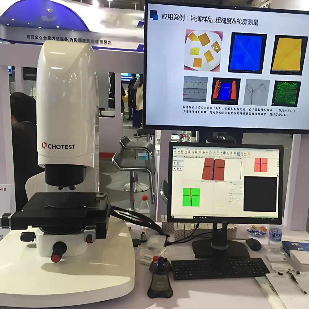
Applications
- Semiconductor manufacturing: Post-CMP surface roughness verification, trench depth profiling, lithography mask defect topography, and wafer bow/warp mapping per SEMI standards
- Optical component metrology: Quantification of polishing-induced subsurface damage, coating uniformity on laser mirrors, and aspheric deviation of IR lenses
- Consumer electronics QA: Glass cover lens haze correlation, metal chassis micro-scratch depth analysis, and OLED encapsulation layer step-height uniformity
- Automotive & MEMS: Gear tooth wear volume calculation, fuel injector nozzle orifice geometry, and pressure sensor diaphragm deflection characterization
- Academic & national lab research: Thin-film growth morphology tracking, graphene layer counting, and nanoscale tribological wear mapping
FAQ
What is the maximum lateral field of view achievable with the standard 10× objective?
The standard 10× interference objective provides a 110 × 82 µm field of view at full resolution; larger areas are covered via automated image stitching with sub-pixel registration accuracy.
Does the system support traceable calibration against NIST-traceable artifacts?
Yes—calibration kits include certified step-height standards (100 nm–10 µm), roughness reference samples (Ra 0.5–50 nm), and flatness references compliant with ISO 5725 and NIST SRM 2100 series.
Can measurement scripts be automated for unattended operation in production environments?
Yes—XtremeVision Pro supports Python API integration and built-in macro recording for fully automated batch routines, including autofocus, region-of-interest selection, parameter extraction, and report generation.
Is the system compatible with cleanroom Class 100 / ISO 5 environments?
The W412 base configuration meets ISO 14644-1 Class 5 particulate limits when operated with optional HEPA-filtered air purge; full cleanroom integration requires custom enclosure design.
How is thermal drift compensated during extended Z-scan acquisitions?
Real-time interferogram phase tracking combined with embedded Pt100 temperature sensors and adaptive focus correction algorithms maintain axial stability within ±0.2 nm over 2-hour continuous scans.


