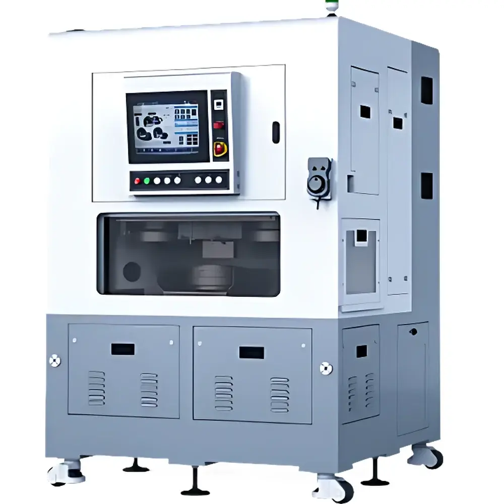
Mengqi Customized Wafer Thinning Machine Model customized-20
| Brand | Mengqi |
|---|---|
| Origin | Imported |
| Manufacturer Type | Authorized Distributor |
| Wafer Size Capacity | 8-inch |
| Grinding Wheel OD | 203 mm |
| Spindle Speed Range | 0–6000 rpm |
| Chuck Rotation Speed | 0–400 rpm |
| Z-Axis Stroke | 130 mm |
| Z-Axis Feed Rate | 0.1–1000 µm/sec (optional down to 0.01 µm/sec) |
| In-situ Thickness Measurement Resolution | 0.1 µm |
| In-situ Thickness Repeatability | ±0.001 mm |
| Material Compatibility | Si, GaAs, SiC, GaN, Sapphire, and other brittle semiconductor substrates |
| Customization | Fully configurable chuck, coolant delivery, metrology integration, and process recipe management |
Overview
The Mengqi Customized Wafer Thinning Machine Model customized-20 is a precision backgrinding system engineered for semiconductor front-end and advanced packaging processes. It employs controlled abrasive grinding—based on deterministic material removal via diamond-impregnated or resin-bonded grinding wheels—to reduce the thickness of processed wafers while maintaining nanoscale thickness uniformity, global flatness (≤0.5 µm TTV), and subsurface integrity. Unlike lapping or etching-based thinning methods, this machine delivers deterministic, repeatable removal rates with real-time thickness feedback, making it suitable for high-yield production of thinned wafers destined for wafer-level packaging (WLP), 3D IC stacking, fan-out redistribution layers (RDL), and MEMS device fabrication. The system operates under cleanroom-compatible environmental controls and integrates seamlessly into automated fab environments via SECS/GEM protocol support.
Key Features
- Precision Z-axis motion control: High-resolution linear motor-driven Z-stage with programmable feed rates from 0.1 µm/sec up to 1000 µm/sec—and optionally down to 0.01 µm/sec—enabling fine-tuned depth-of-cut control for ultra-thin (<50 µm) and stress-sensitive substrates such as SiC and GaN.
- In-situ metrology integration: Non-contact optical interferometric or capacitive thickness sensor mounted directly in the grinding chamber provides real-time, sub-micron resolution (0.1 µm) thickness monitoring with repeatability of ±0.001 mm, supporting closed-loop process correction and endpoint detection.
- Multi-material compatibility: Optimized for silicon, gallium arsenide (GaAs), silicon carbide (SiC), gallium nitride (GaN), sapphire, and quartz substrates—each requiring distinct wheel selection, coolant chemistry, and kinematic parameters to suppress chipping, microcracking, and subsurface damage.
- Modular chuck design: Vacuum chucks with customizable porosity distribution, thermal regulation (±0.5 °C), and edge-guard geometry accommodate 8-inch wafers and support full-face or edge-supported mounting strategies per JEDEC JEP170 and SEMI F57 standards.
- Robust mechanical architecture: Granite base, hydrostatic or preloaded roller guideways, and vibration-damped spindle housing minimize dynamic error sources, ensuring long-term stability over >10,000 hours of continuous operation without recalibration.
- Process traceability & compliance readiness: Embedded logging captures all operational parameters—including wheel wear compensation, coolant flow rate, temperature gradients, and thickness deviation history—with audit trails aligned to ISO 9001, IATF 16949, and FDA 21 CFR Part 11 requirements when paired with validated software packages.
Sample Compatibility & Compliance
The customized-20 supports standard and emerging semiconductor substrate materials used across logic, memory, power electronics, and photonics applications. Its mechanical and thermal tuning enables safe thinning of high-bandgap materials including 4H-SiC (up to 200 mm diameter), AlN-on-Si templates, and III–V heterostructures—all subject to strict surface roughness (Ra < 0.5 nm post-polish) and warp control (≤10 µm bow). Process recipes are compliant with SEMI E10 (Definition of Equipment Reliability), SEMI E142 (Wafer Backside Contamination Control), and ASTM F39 (Standard Test Method for Total Thickness Variation of Silicon Wafers). For automotive-grade devices, the system meets AEC-Q200 stress test prerequisites when configured with redundant coolant filtration and particle-count monitoring.
Software & Data Management
Control is managed through a real-time Linux-based HMI with deterministic scheduling (≤1 ms loop cycle), supporting G-code-style grinding path programming and adaptive algorithm libraries for variable feed-rate profiling. All process data—including thickness maps, wheel wear compensation logs, and thermal drift records—are stored in SQLite or OPC UA-compliant databases. Optional integration with MES platforms (e.g., Applied Materials EnduraLink, PDF Solutions Exensio) enables SPC charting, yield correlation analysis, and automated recipe push-down from engineering workbenches. Software validation documentation—including IQ/OQ/PQ protocols, cybersecurity hardening reports (IEC 62443-3-3), and electronic signature modules—is available upon request for regulated environments.
Applications
- Backgrinding of 8-inch silicon wafers prior to through-silicon via (TSV) formation in 3D NAND and high-bandwidth memory (HBM) stacks.
- Thickness reduction of GaAs RF wafers for millimeter-wave phased-array antenna modules, preserving piezoelectric integrity and minimizing acoustic wave scattering.
- Pre-thinning of SiC power device wafers (650 V–1700 V class) to ≤100 µm for improved thermal resistance and reduced package inductance in EV traction inverters.
- Edge-trim and backside planarization of sapphire substrates used in GaN-on-sapphire LED epitaxy, enabling uniform current spreading and enhanced light extraction efficiency.
- Research-scale thinning of novel 2D material heterostructures (e.g., MoS₂/h-BN/graphene stacks) using low-force, low-heat grinding modes to preserve interfacial van der Waals bonding.
FAQ
What wafer diameters does the customized-20 support?
The standard configuration supports 8-inch (200 mm) wafers. With custom chuck and kinematic reconfiguration, it can be adapted for 6-inch or 12-inch formats—subject to structural validation and metrology recalibration.
Is the system compatible with dry grinding or only wet grinding?
It is designed for aqueous-based coolant delivery systems meeting SEMI F57 purity specifications (particle count <100 particles/mL @ ≥0.5 µm); dry grinding is not supported due to thermal and particulate contamination risks.
Can the machine perform dicing-before-grinding (DBG) alignment?
Yes—when equipped with integrated top-side alignment optics and pattern recognition software, it supports DBG workflows with alignment accuracy ≤±1.5 µm relative to scribe lanes.
Does Mengqi provide process development support?
Yes—application engineers offer joint process qualification at customer sites, including wheel selection matrices, coolant formulation guidance, and DOE-based optimization of removal rate vs. surface quality trade-offs.
How is maintenance access structured for critical components like the spindle and Z-axis drive?
Front-access modular design allows full spindle replacement within 4 hours; Z-axis linear motor and encoder assemblies are field-swappable with calibrated position restoration via onboard laser interferometer referencing.


