Atometrics AM-7000 Series ER-230 White Light Interferometer for Optical Thin Film Metrology
| Brand | Atometrics |
|---|---|
| Origin | Guangdong, China |
| Manufacturer Type | OEM Manufacturer |
| Regional Classification | Domestic (China) |
| Model | AM-7000 Series ER-230 |
| Pricing | Upon Request |
Overview
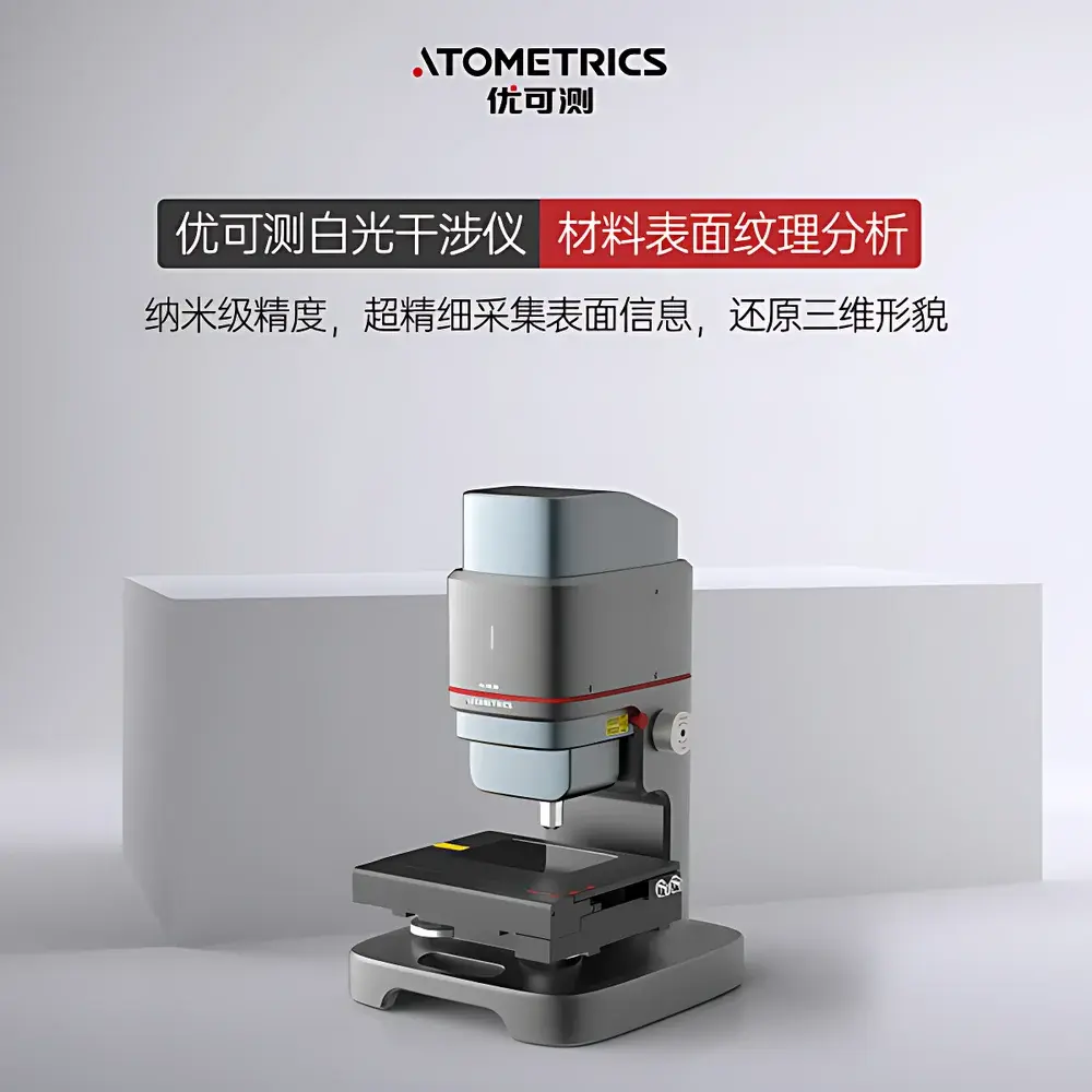
The Atometrics AM-7000 Series ER-230 is a high-precision white light interferometer (WLI) engineered for non-contact, sub-nanometer surface topography and optical thin film characterization. It operates on the principle of low-coherence interferometry, where broadband white light generates localized interference fringes only at the optical path length matching condition—enabling axial resolution independent of objective magnification and immune to chromatic aberration. This architecture delivers traceable vertical resolution down to 0.03 nm (RMS) and lateral resolution governed by the diffraction limit of the selected objective lens (typically 0.5–2.0 µm). Designed specifically for semiconductor process control and advanced optical coating development, the ER-230 variant integrates a high-speed piezoelectric scanning stage capable of linear vertical travel up to 400 µm at velocities exceeding 400 µm/s—ensuring rapid acquisition of full-field 3D surface maps without compromising measurement fidelity. Its metrological stability is maintained across thermal drifts ≤0.1 nm/°C, making it suitable for cleanroom environments compliant with ISO 14644-1 Class 5 or better.
Key Features
- Sub-nanometer vertical resolution (0.03 nm RMS) enabled by proprietary phase-shifting white light interferometry and real-time fringe contrast optimization
- High-speed PZT-driven vertical scanning with programmable scan ranges from 100 nm to 400 µm and maximum velocity of 400 µm/s
- Dedicated optical path configuration optimized for transparent and semi-transparent thin film stacks—including SiO₂, SiNₓ, ITO, Ta₂O₅, and multilayer anti-reflective coatings
- Integrated auto-focus and intelligent surface recognition algorithms for robust measurement initiation on patterned wafers, etched trenches, and stepped structures
- Modular objective turret supporting 2.5× to 100× magnifications with calibrated NA values; compatible with long-working-distance and immersion objectives
- Passive vibration isolation base and environmental drift compensation firmware for stable operation in production-grade facilities
Sample Compatibility & Compliance
The ER-230 supports substrates ranging from 2-inch to 300-mm silicon wafers, fused silica optics, sapphire substrates, and flexible polymer films mounted on rigid carriers. It accommodates sample heights up to 150 mm and thicknesses from 0.1 mm to 25 mm. Measurement protocols are aligned with ASTM E2981 (Standard Guide for Use of White Light Interferometry in Surface Texture Analysis), ISO 25178-603 (areal surface texture—particular characteristics of instruments), and SEMI D39 (specification for optical inspection equipment used in semiconductor manufacturing). Data integrity meets GLP/GMP requirements through audit-trail-enabled software logging, user access controls, and electronic signature support per FDA 21 CFR Part 11 when configured with optional validation packages.
Software & Data Management
Controlled via Atometrics’ proprietary MetroStudio™ v5.x platform, the system provides intuitive workflow-driven measurement sequencing, automated report generation (PDF/CSV/XLSX), and batch processing for multi-site wafer mapping. Advanced analysis modules include film thickness extraction via spectral reflectance modeling (based on Fresnel equations), step-height quantification with edge-detection-assisted ROI selection, PV/Ra/Rq/Sk/Sku parameter extraction per ISO 25178-2, and cross-sectional profile stitching for large-area scans. All raw interferograms and processed datasets are stored in vendor-neutral HDF5 format with embedded metadata (wavelength calibration, environmental conditions, operator ID, timestamp), ensuring long-term archival compliance and third-party interoperability.
Applications
- Semiconductor front-end: gate oxide thickness uniformity on logic/foundry wafers; CMP endpoint verification; STI and shallow trench depth profiling
- Optical coating QC: layer thickness and refractive index determination in AR/HR/beam-splitter stacks; defect localization in ion-beam-sputtered films
- MEMS/NEMS fabrication: release etch depth monitoring, membrane flatness assessment, and comb-drive gap verification
- Advanced packaging: under-bump metallization (UBM) topography, redistribution layer (RDL) planarity, and TSV sidewall roughness
- Research & development: in-situ thin film growth kinetics monitoring (with environmental chamber integration), stress-induced curvature analysis of deposited layers
FAQ
What film thickness range can the ER-230 accurately measure?
The system supports single-layer and multi-layer optical film thickness measurements from ~10 nm to >10 µm, depending on material dispersion, substrate reflectivity, and coherence envelope width.
Does the instrument support automated wafer handling?
Yes—when integrated with standard SECS/GEM-compliant load ports and robotic handlers, the ER-230 enables unattended 300-mm wafer metrology with recipe-based site navigation and statistical process control (SPC) output.
Can MetroStudio™ export data to factory MES systems?
Yes—via configurable OPC UA or SECS-II interfaces, including S2/S8 message sets for tool status, measurement results, and alarm reporting.
Is NIST-traceable calibration available?
Atometrics offers optional annual calibration services certified to ISO/IEC 17025, including step-height standards (NIST SRM 2150a), roughness artifacts (NIST SRM 2161), and wavelength reference filters.
How is environmental sensitivity mitigated during long-duration scans?
Real-time air refractive index compensation is performed using integrated temperature, pressure, and relative humidity sensors; combined with closed-loop PZT position feedback and drift-correction algorithms applied during post-processing.


