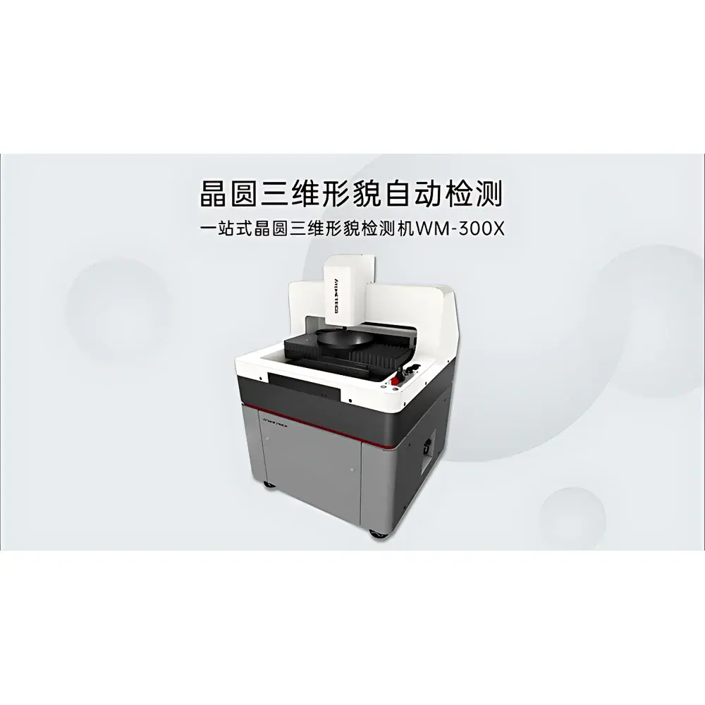
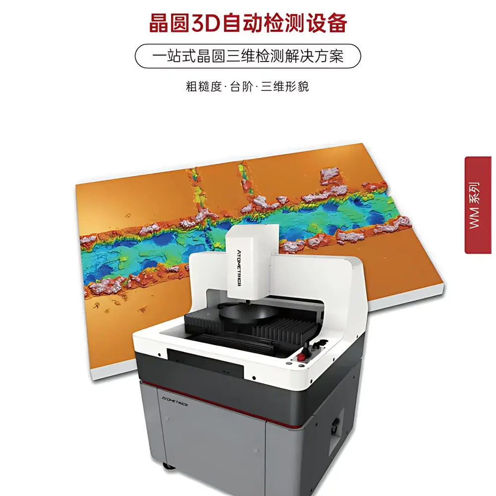
Atometrics WM300X Integrated Wafer Surface Metrology System
| Brand | Atometrics |
|---|---|
| Origin | Guangdong, China |
| Manufacturer Type | OEM/ODM Manufacturer |
| Country of Origin | China |
| Model | WM300X |
| Pricing | Upon Request |
Overview
The Atometrics WM300X Integrated Wafer Surface Metrology System is a non-contact, white-light interferometric (WLI) profiler engineered for high-precision 3D surface topography characterization of semiconductor wafers and photomasks. Leveraging vertical scanning interferometry (VSI) with phase-shifting capabilities, the system delivers nanoscale vertical resolution and sub-nanometer repeatability in height measurements—critical for process control in front-end-of-line (FEOL) and back-end-of-line (BEOL) fabrication steps. Designed specifically for silicon wafer manufacturing workflows—including grinding & thinning, etching, scribing, bumping, and mask inspection—the WM300X supports full-wafer metrology across 4-inch to 12-inch substrates without manual repositioning. Its architecture integrates optical, mechanical, and computational subsystems into a single platform compliant with cleanroom-compatible operational standards (ISO Class 5 compatible housing, VC-D grade vibration isolation).
Key Features
- White-light interferometric measurement engine with 0.03 nm vertical resolution, enabling traceable quantification of surface roughness parameters including Sq (root-mean-square height) and Sa (arithmetic mean height), as validated by reference measurements yielding Sq = 0.714 nm and Sa = 0.572 nm.
- Multi-range piezoelectric Z-scanner offering selectable travel spans of 400 µm or 5000 µm, supporting both fine-scale texture analysis and macro-scale step-height profiling with ±0.3% accuracy up to 5000 µm step heights.
- Modular interference objectives with magnifications of 2.5×, 5×, 10×, 20×, 50×, and 100×, providing flexible trade-offs between field-of-view (up to 1.2 mm × 0.75 mm at 2.5×) and lateral resolution (down to ~0.6 µm at 100×).
- High-speed scientific-grade monochrome CMOS camera (1920 × 1200 pixels, 2.3 MP), optimized for low-noise, high-dynamic-range capture at frame rates from 169 Hz to 3200 Hz, enabling rapid data acquisition even during dynamic scanning.
- Motorized vacuum chuck platform with one-touch vacuum activation, accommodating wafers from 100 mm (4″) to 300 mm (12″) diameter; equipped with VC-D class passive vibration isolation and linear motor-driven XY stage capable of 300 mm/s maximum traverse speed.
Sample Compatibility & Compliance
The WM300X is validated for quantitative surface analysis of polished silicon wafers, fused silica photomasks, copper and nickel bump structures, and dielectric thin films used in advanced packaging. All reported roughness metrics comply with international standards ISO 25178-2:2012 (areal surface texture) and ISO 4287:1997 (profile-based roughness). The system’s measurement algorithms—including SST (Smart Scan Technology) and GAT (Gradient-Aware Thresholding)—are implemented to meet statistical process control (SPC) requirements in ISO 9001-certified fabs. Data integrity is maintained through audit-trail-enabled software architecture aligned with 21 CFR Part 11 principles for electronic records and signatures where configured per customer validation protocols.
Software & Data Management
The proprietary Atometrics SurfaceAnalyzer™ software provides a unified interface for instrument control, real-time visualization, automated recipe-based measurement, and ISO-compliant reporting. It supports batch processing of multiple sites across a wafer map, cross-sectional profile extraction, power spectral density (PSD) analysis, and defect localization via height deviation thresholding. Raw interferograms and processed topography maps are stored in vendor-neutral formats (e.g., .xyz, .csv, .tif) for integration with factory MES systems or third-party SPC tools. Software calibration routines include NIST-traceable step-height standards and certified roughness reference samples, ensuring long-term measurement stability and inter-laboratory comparability.
Applications
- Silicon rod cutting & wafer slicing: Quantitative assessment of kerf loss, subsurface damage depth, and edge chipping morphology.
- Grinding & thinning processes: In-line monitoring of surface uniformity, waviness, and residual stress-induced deformation.
- Photomask inspection: Characterization of chrome layer thickness variation, character depth (e.g., 0.098 µm), and horizontal feature spacing (e.g., 56.627 µm).
- Etch & deposition uniformity: Step-height mapping across patterned layers to evaluate etch selectivity and film conformality.
- Bumping & redistribution layer (RDL) metrology: Measurement of solder bump height, coplanarity, and interfacial roughness prior to flip-chip bonding.
- Equipment qualification & DOE studies: Rapid comparative evaluation of consumables (e.g., polishing pads, slurries) under controlled experimental conditions.
FAQ
What surface roughness parameters does the WM300X report in compliance with ISO 25178?
It calculates and exports all primary areal parameters defined in ISO 25178-2, including Sa, Sq, Sz, Ssk, Sku, Sdr, and Sal, with optional filtering (Gaussian, robust, spline) applied per ISO 16610-21.
Can the system measure transparent or semi-transparent thin films on silicon?
Yes—using multi-wavelength VSI mode and refractive index input, it resolves film thickness and interface roughness simultaneously for dielectrics such as SiO₂, SiNₓ, and low-k materials.
Is the platform compatible with automated wafer handling systems?
The WM300X supports SECS/GEM communication protocol via optional RS-232/Ethernet interface, enabling integration into cluster tools and automated material handling environments.
How is measurement traceability maintained over time?
Through periodic verification using NIST-traceable step-height standards (e.g., 100 nm–5 µm certified steps) and roughness artifacts, documented in calibration certificates aligned with ISO/IEC 17025 requirements.
Does the software support custom report templates for internal QA documentation?
Yes—SurfaceAnalyzer™ includes a configurable report generator with drag-and-drop fields, company branding, and export to PDF, Excel, or XML for LIMS/MES ingestion.