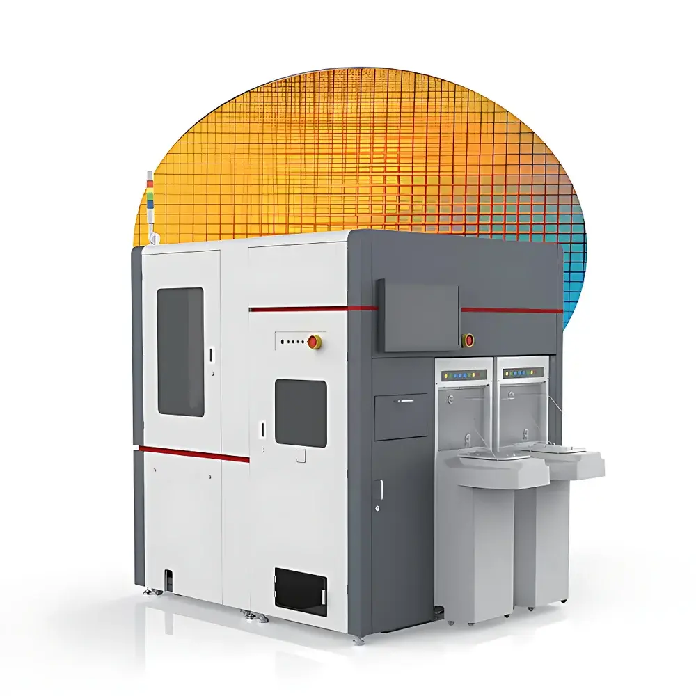
Atometrics WPM Series White-Light Interferometric Wafer 3D Metrology System
| Brand | Atometrics |
|---|---|
| Origin | Guangdong, China |
| Manufacturer Type | OEM Manufacturer |
| Product Category | Domestic |
| Model | WPM Series |
| Pricing | Upon Request |
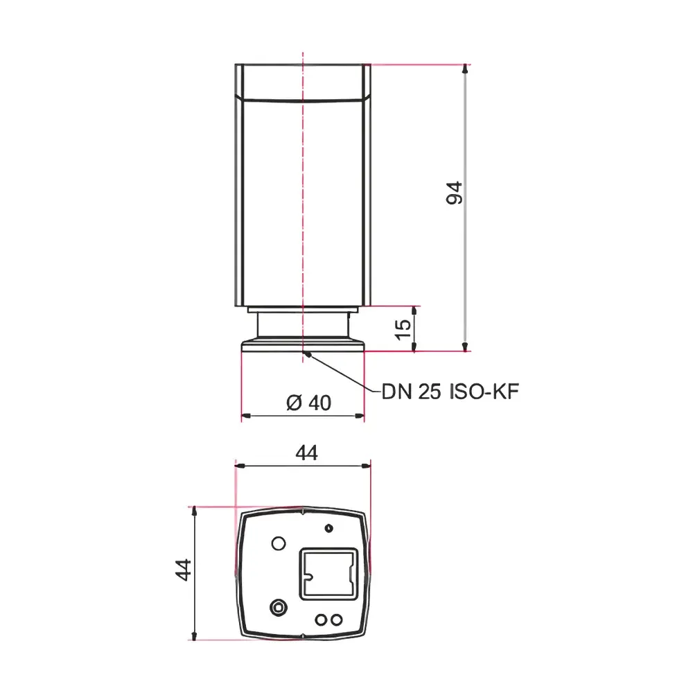
| Instrument Type | Non-Contact Profilometer / Surface Roughness Analyzer |
| Operating Principle | White-Light Interferometry |
| Vertical Resolution | 0.001 nm |
| Surface Topography Repeatability (PSI mode, 3×3 filter, 1M points, Sqj/� | 2): 0.03 nm |
| Step Height Accuracy (12 µm NIST-traceable step standard, n=50) | ±0.3% |
| XY Positional Repeatability | <0.19 µm |
| Maximum Vertical Scan Speed | 400 µm/s |
| Typical Vertical Scan Speed | 35 µm/s |
| Maximum Lateral Resolution | 0.19 µm |
| Multi-Layer Thin-Film Measurement Capability | Up to 10 layers |
| Roughness Standards Compliance | ISO 25178, ISO 4287, ISO 287 |
| Overlay Measurement Support | Custom algorithm-enabled |
| Bump & RDL Profile Reconstruction | Enabled via phase-resolved interferometric imaging |
| CMP Uniformity Analysis | Full-wafer die-level topography mapping with dishing/erosion quantification |
Overview
The Atometrics WPM Series is a research-grade, white-light interferometric (WLI) wafer 3D metrology platform engineered for high-precision, non-contact surface topography and thin-film characterization in semiconductor process development and advanced packaging environments. Unlike laser confocal or focus-variation systems—whose vertical accuracy is constrained by mechanical stage resolution and optical magnification—the WPM Series leverages the intrinsic wavelength-stability of broadband interference to achieve sub-nanometer vertical resolution independent of objective magnification. Its core measurement principle relies on coherence-gated fringe analysis: as a piezoelectric transducer scans the reference mirror through the coherence length of white light, interference fringes are generated only when the optical path difference between sample and reference arms falls within ~1–2 µm. The resulting intensity-modulated signal is processed using fast Fourier transform (FFT)-based phase extraction algorithms to reconstruct height maps with pixel-level fidelity. This physics-based approach ensures traceable, repeatable, and magnification-invariant height metrology across full 200 mm and 300 mm wafer formats.
Key Features
- Sub-angstrom vertical resolution: 0.001 nm system resolution with 0.03 nm topography repeatability under PSI (Phase-Shifting Interferometry) mode—validated per ISO 25178-602 using spatial filtering and statistical point cloud analysis.
- Nanopositioning actuation: High-speed, large-range piezoelectric scanner enabling vertical scan speeds up to 400 µm/s—5× faster than conventional WLI platforms—without sacrificing phase stability or fringe contrast.
- Vibration-compensated optical architecture: Integrated VC-D (Vibration-Controlled Damping) air-isolation system featuring millimeter-precision valve placement and dynamic center-of-mass stabilization; suppresses environmental microvibrations and enables rapid settling (<100 ms) after motion initiation.
- High-NA white-light objective lens: Optimized for broad spectral transmission (400–700 nm), delivering diffraction-limited lateral resolution down to 0.19 µm at 50× magnification.
- Multi-modal measurement engine: Simultaneous acquisition of topography, thin-film thickness (via spectral reflectance modeling), roughness (Sa, Sq, Sz, Ra, Rz, Rq), warpage/bow/stress, and overlay error—within a single scan sequence.
- Automated workflow integration: Scriptable measurement sequencing via Python API; fully programmable stage navigation, focus search, and region-of-interest definition for inline or offline deployment.
Sample Compatibility & Compliance
The WPM Series supports bare and patterned silicon wafers (200 mm, 300 mm), compound semiconductor substrates (GaN, SiC), glass carriers, and advanced packaging substrates including ABF, BT, and RDL structures. It accommodates samples with high aspect-ratio features (e.g., TSVs, micro-bumps), low-reflectivity surfaces (e.g., SiN, TiN), and multi-layer stacks (up to 10 films). All surface texture parameters conform to ISO 25178-2 (areal surface texture), ISO 4287 (profile roughness), and ISO 287 (surface finish notation). Thin-film thickness results are traceable to NIST SRM 1732 and calibrated against ellipsometric references. The system meets GLP-compliant data integrity requirements—including audit trail logging, electronic signature support, and 21 CFR Part 11–ready user access controls—when deployed with optional secure software licensing.
Software & Data Management
Atometrics’ proprietary WPM Control Suite provides unified control over hardware synchronization, real-time fringe visualization, and post-processing analytics. Raw interferogram data is stored in HDF5 format with embedded metadata (timestamp, calibration ID, environmental conditions, operator ID). Advanced analysis modules include: CMP uniformity mapping with die-level dishing/erosion quantification; bump profile reconstruction using curvature-adaptive edge detection; EBR (Edge Bead Removal) width and shape assessment; and overlay error decomposition (X/Y translation, rotation, scaling) via custom fiducial recognition algorithms. All reports export to PDF, CSV, and STEP AP210 for CAD-integrated process feedback loops. Data retention policies, version-controlled script libraries, and role-based permissions ensure compliance with internal QA protocols and external audit frameworks.
Applications
- Semiconductor front-end: Critical dimension (CD) monitoring of etched trenches and vias; gate oxide thickness uniformity; STI height and planarity verification.
- Advanced packaging: Micro-bump height, coplanarity, and solder volume estimation; RDL line width and edge roughness; underfill void detection via topographic depression mapping.
- CMP process control: Full-wafer bow/warpage mapping; local dishing and erosion quantification at die level; slurry selectivity validation via film-thickness-to-topography correlation.
- MEMS & photonics: Mirror flatness certification; grating pitch and sidewall angle measurement; waveguide surface roughness (Sa < 0.1 nm) for low-loss optical coupling.
- Materials R&D: Stress-induced curvature analysis via Stoney equation integration; thin-film adhesion failure detection through localized delamination morphology.
FAQ
What is the vertical measurement uncertainty for step heights under production conditions?
For a 12 µm certified step standard measured under controlled lab conditions (22 ± 0.5 °C, humidity <40% RH), the expanded uncertainty (k=2) for step height is ±0.3% of reading, verified across 50 repeated measurements.
Does the system support automated overlay metrology without manual fiducial alignment?
Yes—custom overlay algorithms identify process-defined alignment marks (e.g., box-in-box, L-shaped targets) and compute translational, rotational, and scaling errors with sub-pixel registration accuracy. Calibration is performed using wafer-level photomask references.
Can the WPM Series measure transparent thin films on opaque substrates?
Yes—spectral reflectance modeling within the software supports multi-layer film stack analysis on Si, SiO₂, SiN, and metal substrates. Up to 10 layers can be simultaneously fitted using Levenberg-Marquardt optimization constrained by Kramers-Kronig consistency.
Is the system compatible with cleanroom Class 100/ISO 5 environments?
The WPM Series chassis is constructed from stainless steel and anodized aluminum; all internal optics are sealed and purged. Optional HEPA-filtered air curtain kits and static-dissipative stage coatings are available for full ISO 5 integration.
How is traceability maintained for factory recalibration?
Each system ships with a NIST-traceable interferometric step standard and documented calibration certificate. On-site recalibration follows ISO/IEC 17025 procedures, with full uncertainty budgets provided in accordance with EURAMET cg-18.