Atometrics AF T010 White Light Interferometric Thin-Film Thickness Measurement System
| Brand | Atometrics |
|---|---|
| Origin | Guangdong, China |
| Manufacturer Type | Manufacturer |
| Product Category | Domestic |
| Model | AF T010 |
| Pricing | Upon Request |
Overview
The Atometrics AF T010 is a high-precision white light interferometric thickness measurement system engineered for non-contact, label-free characterization of thin films and multilayer structures across R&D laboratories, semiconductor process development, and advanced materials manufacturing. Based on spectral reflectometry combined with vertical scanning white light interferometry (WSLI), the AF T010 captures interference fringes generated at film–substrate and interlayer interfaces, enabling quantitative reconstruction of optical thickness (n·d) through rigorous inverse modeling. Unlike conventional single-wavelength ellipsometers or eddy-current gauges, the AF T010 leverages broadband spectral acquisition (180–2400 nm) to resolve complex optical dispersion behavior—particularly critical for transparent conductive oxides (e.g., ITO), perovskite absorbers, quantum dot layers, spin-coated polymers (e.g., PI), and low-k dielectrics (e.g., SiO₂). Its core architecture integrates dual stabilized light sources—a deuterium lamp (180–370 nm) for deep UV sensitivity and a tungsten-halogen lamp (320–2400 nm) for extended NIR coverage—ensuring uniform spectral irradiance and minimizing photometric drift during long-term acquisition.
Key Features
- Sub-angstrom axial resolution (≤0.1 nm theoretical) enabled by high-stability piezoelectric vertical scanning and sub-pixel phase analysis
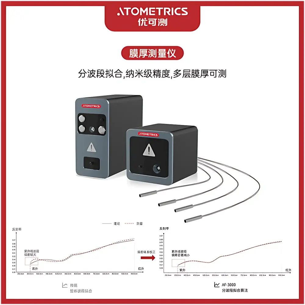
- Multi-band spectral fitting algorithm: replaces global polynomial fitting with segmented spectral domain optimization—reducing UV-region reflectance modeling error by >85% compared to conventional full-spectrum regression
- Support for up to 10-layer stack inversion with simultaneous determination of thickness (d), refractive index (n), and extinction coefficient (k) per layer
- Millisecond-level acquisition speed (<100 ms per spectrum), optimized for inline process monitoring and rapid offline mapping
- Modular configuration options: benchtop offline unit, compact inline OEM module (USB 3.0 interface, footprint <120 × 80 × 60 mm), and fully automated wafer-handling integration (compatible with 100–300 mm substrates)
- Optical path designed for high repeatability under ambient lab conditions—no active temperature stabilization required for ±0.3% thickness reproducibility over 8-hour sessions
Sample Compatibility & Compliance
The AF T010 accommodates a broad range of sample geometries and surface conditions: flat wafers (Si, glass, sapphire), flexible polymer substrates, microfluidic channels, patterned photomasks, and rough or textured coatings (Ra ≤ 50 nm). It supports measurements on liquid films (e.g., spin-coated precursor solutions), air gaps, and buried interfaces without vacuum requirements. All optical models and calibration protocols adhere to ISO/IEC 17025 traceability principles. Software includes audit-trail logging compliant with FDA 21 CFR Part 11 for regulated environments; raw spectral data export conforms to ASTM E2982-21 (Standard Guide for Spectral Reflectance Measurements of Thin Films) and supports GLP/GMP documentation workflows.
Software & Data Management
The proprietary Atometrics ThinFilm Studio v4.x platform provides full control over acquisition parameters, real-time spectral preview, multi-layer optical model building (Cauchy, Sellmeier, Tauc-Lorentz dispersion functions), and iterative Levenberg-Marquardt fitting. Batch processing supports spatial mapping (line scans, area grids), statistical thickness uniformity reporting (±3σ, %CV), and cross-platform data exchange via HDF5 and CSV. Version-controlled method templates ensure inter-laboratory consistency. For production integration, RESTful API and OPC UA support enable seamless connectivity with MES/SCADA systems and SPC dashboards.
Applications
- Semiconductor: thickness and uniformity verification of ALD/CVD-grown high-k dielectrics (HfO₂, Al₂O₃), gate oxides, and metal nitride barriers
- Photovoltaics: in-line monitoring of perovskite absorber layers (18–50 nm), HTL/ETL stacks (NiOₓ, SnO₂), and anti-reflective coatings
- Display & Optoelectronics: QC of ITO (10–20 nm), quantum dot color conversion films (35–100 nm), and encapsulation barrier layers (SiNₓ, Al₂O₃)
- MEMS & Microfluidics: quantification of channel depth (3–5 µm), bonding interface integrity, and sacrificial layer removal endpoints
- Advanced Packaging: thickness mapping of redistribution layers (RDLs), under-bump metallization (UBM), and fan-out wafer-level packaging (FOWLP) dielectrics
FAQ
What is the minimum measurable thickness for single-layer transparent films?
The practical lower limit is ~1 nm for high-contrast interfaces (e.g., SiO₂ on Si), governed by signal-to-noise ratio and dispersion modeling stability—not instrument resolution alone.
Does the system require reference standards for calibration?
No primary thickness standards are needed; calibration relies on built-in wavelength reference lines (Hg/Ar emission peaks) and air-gap zero-order fringe detection for absolute optical path difference alignment.
Can it measure films on curved or non-planar substrates?
Yes—via motorized tilt compensation and focus-tracking algorithms; maximum substrate curvature radius supported: 25 mm.
Is the software validated for use in regulated pharmaceutical or medical device manufacturing?
Yes—ThinFilm Studio v4.x includes 21 CFR Part 11-compliant electronic signatures, role-based access control, and immutable audit trails for IQ/OQ/PQ documentation.
How does the segmented spectral fitting improve accuracy over traditional methods?
By partitioning the spectrum into physically meaningful bands (UV, visible, NIR), the algorithm applies distinct dispersion models per region—mitigating cross-band parameter correlation and significantly reducing residual error in UV-sensitive materials like ITO and perovskites.


