ZENO QUASAR-S Series Industrial In-Line Optical Thin Film Metrology System
| Brand | ZENO |
|---|---|
| Model | QUASAR-S Series |
| Application | In-line optical metrology for semiconductor wafer fabrication |
| Wafer Sizes | 150 mm (6″), 200 mm (8″), 300 mm (12″) |
| Measurement Principle | Spectroscopic Ellipsometry (SE) and Spectral Reflectometry (SR) |
| Spectral Range | UV–Vis–NIR (e.g., 190–1700 nm) |
| Thickness Resolution | ≤ 0.005 nm (3σ) |
| Throughput | Up to 120 wafers/hour |
| Sample Interfaces | Open cassette, SMIF pod, FOUP |
| Measurement Capabilities | Single-layer & multi-layer film thickness, refractive index (n), extinction coefficient (k), patterned & unpatterned wafer alignment, waferless recipe setup |
| Compliance | Designed for integration into ISO Class 1–5 cleanroom environments |
| Software | ZENO MetroSuite™ with audit trail, user access control, and 21 CFR Part 11–compliant electronic records |
Overview
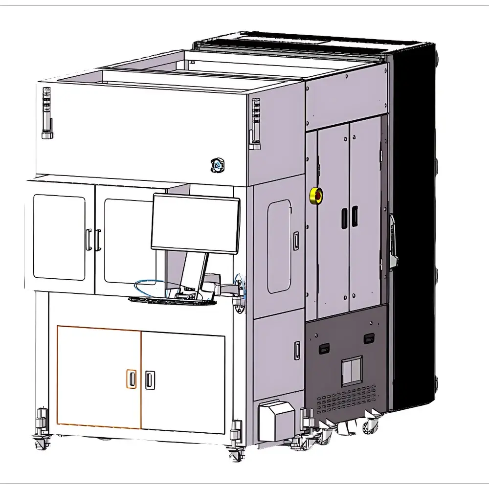
The ZENO QUASAR-S Series is an industrial in-line optical thin film metrology system engineered for real-time, non-contact thickness and optical constant characterization of dielectric, metallic, and compound semiconductor films during integrated circuit (IC) manufacturing. Leveraging dual-mode spectroscopic ellipsometry (SE) and spectral reflectometry (SR), the system delivers nanoscale resolution across ultraviolet, visible, and near-infrared wavelengths (190–1700 nm). Its architecture is purpose-built for high-volume semiconductor fabs—supporting 150 mm, 200 mm, and 300 mm wafers—including advanced substrates such as silicon carbide (SiC) and sapphire-based MicroLED wafers. Unlike offline benchtop tools, the QUASAR-S integrates directly into track or cluster tool environments via standard mechanical and electrical interfaces, enabling closed-loop process control without disrupting line throughput. The system operates under ISO Class 1–5 cleanroom conditions and conforms to SEMI E10 (Specification for Definition and Measurement of Equipment Reliability, Maintainability, and Availability), SEMI E11 (Equipment Communication Standard), and SEMI E142 (Factory Automation Interface Standard) requirements.
Key Features
- Dual-technology measurement engine combining spectroscopic ellipsometry (SE) and spectral reflectometry (SR) for robust n/k and thickness extraction across single-layer and complex multi-layer stacks (e.g., SiO₂/SiNₓ/TiN or AlGaN/GaN heterostructures)
- Nanometer-class precision: thickness repeatability ≤ 0.005 nm (3σ) on reference SiO₂ films, validated per ASTM F398 and ISO/IEC 17025 traceable protocols
- High-throughput design: fully automated handling supporting up to 120 wafers per hour with sub-second measurement cycle time per site
- Multi-interface compatibility: native support for open cassettes, SMIF pods, and FOUPs with vacuum-compatible load ports and robotic end-effector alignment
- Advanced pattern recognition: AI-accelerated vision algorithms enable accurate site localization on patterned wafers—even at sub-10 µm feature pitches—without reliance on pre-defined alignment marks
- Waferless recipe development: allows full optical model calibration and measurement parameter optimization using reference substrates or virtual wafer templates, reducing qualification time by >40% versus traditional methods
- Unpatterned wafer capability: utilizes edge-detection and centroid-based navigation for precise metrology positioning on bare or lightly polished substrates (e.g., SiC boules or GaN-on-sapphire blanks)
Sample Compatibility & Compliance
The QUASAR-S accommodates industry-standard semiconductor substrates including silicon, SOI, SiC, GaN, sapphire, and fused quartz. It supports both front-side and back-side measurements with optional motorized tilt compensation. All optical modules are sealed and particle-controlled per ISO 14644-1 Class 5 specifications. Mechanical integration complies with SEMI E10 reliability benchmarks (MTBF ≥ 5,000 hours) and EHS guidelines for Class 100 cleanroom operation. Electrical safety meets IEC 61000-6-2/6-4 and UL 61010-1. Data integrity adheres to FDA 21 CFR Part 11 requirements through ZENO MetroSuite™’s role-based access control, electronic signature workflows, and immutable audit trails.
Software & Data Management
ZENO MetroSuite™ is a Windows-based, GMP-aligned metrology software platform featuring real-time SPC charting, multi-tool data aggregation, and recipe version control. It provides full GLP/GMP traceability—including instrument calibration history, operator logs, environmental sensor records (temperature, humidity), and raw spectrum archiving. Integration with factory-level MES and APC systems is achieved via SECS/GEM-compliant communication stacks. All measurement data is stored in vendor-neutral HDF5 format, enabling third-party analysis with Python, MATLAB, or JMP. Software validation documentation (IQ/OQ/PQ protocols) is available upon request for regulated environments.
Applications
- Gate oxide and high-k dielectric monitoring in CMOS FEOL processes
- Hard mask and ARC thickness control in lithography stacks
- Epitaxial layer verification for RF and power devices (e.g., GaN HEMTs)
- Passivation film uniformity assessment (SiNₓ, SiO₂) post-packaging
- MicroLED pixel stack metrology (ITO/DBR/Alq₃) on sapphire or glass carriers
- In-line qualification of ALD and PECVD deposition tools via run-to-run feedback
FAQ
What wafer sizes does the QUASAR-S support?
The system is configured for 150 mm, 200 mm, and 300 mm wafers, with interchangeable chuck assemblies and vision calibration profiles.
Can it measure transparent conductive oxides like ITO on flexible substrates?
Yes—when equipped with extended NIR optics and appropriate modeling libraries, it quantifies thickness and carrier concentration in TCO layers on PET, PI, or glass.
Is remote diagnostics and software update supported?
ZENO MetroSuite™ includes secure TLS-encrypted remote support mode compliant with ISO/IEC 27001, enabling firmware updates and troubleshooting without physical access.
How is calibration maintained in high-utilization fabs?
The system features automated daily self-calibration using NIST-traceable reference standards; full recalibration intervals are defined per ISO/IEC 17025 and typically scheduled every 6 months or after 1,000 measurement cycles.
Does it support DOE-driven recipe optimization?
Yes—integrated Design of Experiments (DOE) module enables statistical variation analysis across film stack parameters, linking metrology output directly to process inputs for APC model training.


