Abner ABN-PRO-001 Fully Automated Probe Station
| Brand | Abner |
|---|---|
| Origin | Jiangsu, China |
| Model | ABN-PRO-001 |
| Operation Type | Fully Automatic |
| Platform Size | 60 cm × 60 cm |
| XY Travel Range | 50 mm × 50 mm |
| Z Travel | 200 mm |
| Max Sample Size | 65 mm × 65 mm |
| Max Sample Weight | 4 kg |
| CCD Magnification Options | 5×, 10×, 20×, 50× (long-working-distance objective) |
| Vertical Speed Range | 0.02–4 mm/s |
| Rotation | 360° motorized |
| Illumination | Coaxial ring + transmitted backlight |
| Control Interface | Integrated touchscreen (780 mm × 600 mm display), software-driven with manual override capability |
| Environmental Operating Range | 0–40 °C, ≤80% RH |
Overview
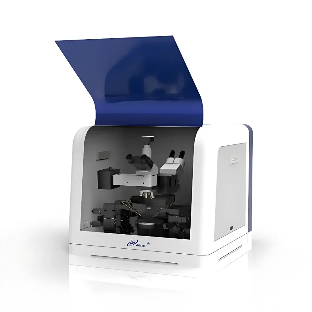
The Abner ABN-PRO-001 Fully Automated Probe Station is an engineered solution for precision electrical characterization of microscale and nanoscale semiconductor devices under controlled laboratory or pilot-line conditions. Built upon a rigid optical-grade granite platform, the system implements a closed-loop XYZθ motion architecture—comprising high-resolution stepper motors, linear encoders, and backlash-free lead-screw mechanisms—to deliver repeatable sub-micron positioning accuracy. Its core measurement paradigm supports DC I-V, AC C-V, pulsed IV, and low-current leakage analysis when interfaced with external parameter analyzers (e.g., Keysight B1500A, Keithley 4200-SCS) via standard GPIB, USB-TMC, or Ethernet-based SCPI protocols. Designed explicitly for wafer-level probing without vacuum or cryogenic requirements, the ABN-PRO-001 serves as a foundational platform for process development, device validation, and failure analysis in both academic cleanrooms and semiconductor R&D labs.
Key Features
- Fully motorized XYZθ positioning system with programmable speed profiles and absolute position retention across power cycles
- Automated probe touchdown detection and force-limited contact control to minimize pad damage and ensure consistent contact resistance
- Modular probe holder design supporting up to four independently actuated tungsten or铍-copper probes (standard 10 µm–50 µm tip diameters), configurable for differential, Kelvin, or multi-terminal measurements
- Integrated long-working-distance microscope with motorized zoom turret and dual illumination modes (coaxial ring light for surface topography; transmitted backlight for transparent substrates)
- Real-time image registration and pattern-matching algorithm for automated die alignment—capable of recognizing fiducials, bond pads, or lithographic markers with ≤1.5 µm registration uncertainty
- Hardware-enforced safety interlocks including emergency stop circuitry, mechanical end-stop limit switches, and software-defined virtual boundaries to prevent collision during automated sequences
Sample Compatibility & Compliance
The ABN-PRO-001 accommodates standard semiconductor wafers (up to 150 mm diameter), diced dies on carriers, MEMS packages, and 2D material flakes transferred onto Si/SiO₂ or quartz substrates. Vacuum chucks (optional) and thermal stages (−40 °C to +150 °C, optional) extend compatibility to temperature-dependent characterization. All motion controllers comply with IEC 61800-5-1 for adjustable-speed electrical power drive systems. The control software architecture supports audit trail logging and user access levels aligned with GLP and ISO/IEC 17025 documentation requirements. While not FDA-certified, the system’s deterministic operation and traceable calibration procedures meet common internal QA criteria for pre-production qualification testing per JEDEC JESD22-A114 and A118 standards.
Software & Data Management
AbnerProbeControl™ v3.2 provides a unified interface for hardware orchestration, script-based test sequencing (Python API included), and real-time waveform visualization. Users define measurement routines—including coordinate mapping, probe approach logic, parameter analyzer synchronization, and pass/fail thresholds—via intuitive graphical workflow editors. All acquired data are timestamped and stored in HDF5 format with embedded metadata (sample ID, probe configuration, environmental readings, operator login). Export modules support CSV, MATLAB .mat, and SPICE-compatible netlist generation. Optional integration with LabArchives ELN or Benchling enables direct experimental record linkage. Audit logs capture every command execution, parameter change, and hardware state transition—fully compliant with 21 CFR Part 11 electronic signature requirements when deployed with Windows domain authentication.
Applications
- Parametric testing of front-end-of-line (FEOL) transistors and back-end-of-line (BEOL) interconnect structures during process integration
- Reliability stress testing (HTOL, TDDB, NBTI) using synchronized voltage ramping and leakage monitoring
- Contact resistance extraction and transmission line method (TLM) analysis for novel electrode stacks
- Electrostatic discharge (ESD) robustness screening of RF and power devices via TLP pulse injection
- In situ electrical characterization of graphene, MoS₂, and other 2D heterostructures under ambient or inert gas environments
- MEMS switch actuation cycling and contact resistance drift analysis over 10⁵+ cycles
FAQ
Does the ABN-PRO-001 support cryogenic or vacuum operation?
No—the base configuration operates at ambient pressure and temperature. Cryogenic stages (down to 4 K) and vacuum chambers (10⁻⁶ mbar) are available as validated third-party integrations but require mechanical and electrical interface redesign.
Can the system be integrated with existing parameter analyzers from Keysight or Keithley?
Yes—native SCPI command sets for both vendors are preloaded; custom drivers can be developed for other instruments upon request.
Is remote operation supported over LAN or VPN?
Yes—full GUI mirroring and script execution are enabled via RDP or VNC; TLS-encrypted REST API access is available for enterprise automation pipelines.
What calibration services are offered?
Abner provides annual positional verification (traceable to NIST standards) and optional electrical calibration of onboard encoders and limit sensors.
How is probe wear monitored during extended unattended runs?
The software tracks cumulative touchdown cycles per probe and triggers maintenance alerts based on user-defined thresholds; optional vision-based tip degradation analysis is available as an add-on module.


