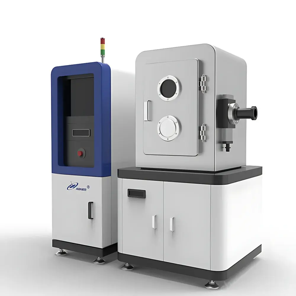
Abner ABN EBL Series Electron Beam Lithography System
| Brand | Abner |
|---|---|
| Origin | Jiangsu, China |
| Manufacturer Type | Authorized Distributor |
| Country of Origin | China |
| Model | ABN EBL Series |
| Component Category | Electron Optics Subsystem |
| Pricing | Upon Request |
Overview
The Abner ABN EBL Series Electron Beam Lithography (EBL) System is a high-precision, direct-write nanofabrication instrument engineered for research-grade micro- and nanoscale patterning. Operating on the principle of focused electron beam scanning in ultra-high vacuum (UHV), the system exploits the short de Broglie wavelength of accelerated electrons (typically 1–30 keV) to bypass the optical diffraction limit inherent in photolithography. This enables deterministic, maskless exposure of electron-sensitive resists—such as PMMA, HSQ, and ZEP—with sub-10 nm critical dimension (CD) resolution and positional accuracy better than ±2 nm (3σ). Designed for integration into cleanroom-based nanofabrication workflows, the ABN EBL system delivers deterministic pattern fidelity across substrates including silicon wafers, GaAs, quartz, glass, and 2D material heterostructures. Its architecture conforms to fundamental requirements for reproducible nanoscale process development: stable electron optics, calibrated dose control, real-time beam blanking, and metrology-aware stage positioning.
Key Features
- Sub-10 nm resolution capability with verified line-width control down to 8 nm (FWHM) on standard PMMA/950K resist stacks
- Integrated electron optical column featuring thermionic or Schottky field-emission source, doublet/multiplet condenser and objective lenses, and dynamic stigmator compensation
- 50 MHz digital pattern generator with 20 ns minimum pixel dwell time and dual 16-bit DACs for X/Y beam deflection
- High-stability mechanical platform with active vibration isolation and thermal drift compensation (<0.5 nm/min at 23 ± 0.1 °C)
- Full compatibility with industry-standard CAD data formats: GDSII, OASIS, and DXF with layer mapping and hierarchical flattening
- Vacuum interlocked chamber (base pressure <5×10⁻⁷ mbar) with automated load-lock and residual gas analyzer (RGA) monitoring
- Dose modulation engine supporting proximity effect correction (PEC), variable-shape beam (VSB) stitching, and multi-pass exposure sequencing
Sample Compatibility & Compliance
The ABN EBL system accommodates substrates up to 4-inch diameter (standard) with optional 6-inch upgrade. Compatible materials include Si/SiO₂, SOI, GaAs, InP, sapphire, fused silica, and transferable 2D membranes (graphene, h-BN, MoS₂). Resist processing supports both positive-tone (PMMA, copolymers) and negative-tone (HSQ, ZEP-520A) chemistries, with bake and development protocols aligned to SEMI and ISO 14644-1 Class 4 cleanroom standards. The system’s operational software logs all exposure parameters—including beam energy, current, dwell time, and stage coordinates—with timestamped audit trails compliant with GLP and internal R&D documentation requirements. While not certified for FDA 21 CFR Part 11, its data export architecture (CSV, HDF5, XML) supports traceability frameworks required for academic publication and patent documentation.
Software & Data Management
The ABN EBL Control Suite is a native Windows-based application tightly integrated with SEM imaging environments—enabling seamless transition between inspection and lithography modes. It features a modular GUI with dedicated modules for layout import, proximity correction modeling (using Monte Carlo-based algorithms), alignment mark detection (via secondary electron contrast), and recipe-driven batch execution. All exposure jobs are stored in a relational database with versioned project histories. Raw beam position data, dose maps, and stage trajectory logs are archived automatically. Export options include calibrated TIFF overlays for overlay metrology, JSON-formatted parameter sets for cross-platform process replication, and GDSII derivatives for foundry handoff. Remote operation via secure TLS-encrypted VNC is supported for collaborative lab environments.
Applications
- Prototyping of advanced semiconductor devices: FinFET test structures, tunnel FETs, and nanowire transistors requiring sub-20 nm gate definition
- Fabrication of quantum devices: Josephson junction arrays, superconducting qubit capacitors, and electrostatically defined quantum dots in GaAs/AlGaAs heterostructures
- Nanophotonic and plasmonic components: Aperiodic metasurfaces, Yagi-Uda nanoantennas, and photonic crystal cavities with Q > 10⁴
- 2D material device engineering: Edge-contact electrodes for graphene Hall bars, split-gate constrictions in TMD monolayers, and van der Waals heterostructure alignment marks
- Materials science templates: Nanoporous anodized alumina masks, colloidal lithography masters, and sacrificial lift-off scaffolds for epitaxial growth
FAQ
What vacuum level is required for stable operation?
The system requires a base pressure ≤5×10⁻⁷ mbar in the main chamber, achieved using a combination of turbomolecular pumping and ion gettering. Load-lock evacuation to 10⁻⁵ mbar is sufficient for wafer transfer.
Is the system compatible with cryogenic stages?
Yes—optional liquid-helium or closed-cycle cryostat integration is available for low-temperature lithography (4–77 K), enabling strain-tuned 2D material patterning and superconducting device fabrication.
How is beam current calibrated and maintained?
Beam current is measured in real time using a Faraday cup with NIST-traceable calibration. Automatic current stabilization is achieved via feedback-controlled Wehnelt bias modulation, with drift <±0.5% over 8-hour runs.
Can the system perform multi-layer alignment?
Yes—using fiducial-based alignment with sub-5 nm registration repeatability (3σ), supported by in-situ SEM imaging and automated cross-correlation algorithms.
What maintenance intervals are recommended?
Filament replacement every 1,200–1,800 hours; stigmator recalibration quarterly; vacuum pump oil change biannually; full electron optical alignment annually per ISO/IEC 17025 guidelines.


