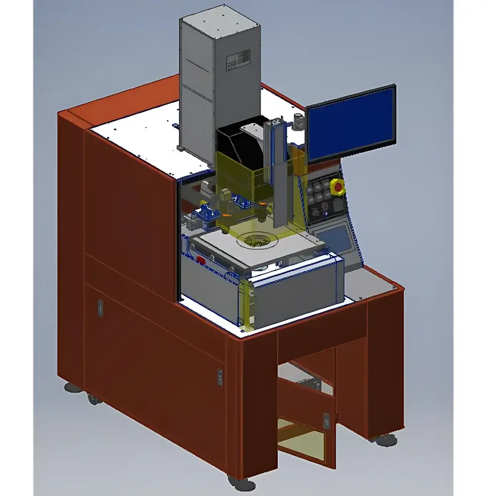
M&R AA-8N-LED Contact Lithography and Bond Alignment Integrated System
| Brand | M&R |
|---|---|
| Origin | Taiwan |
| Model | AA-8N-LED |
| Light Source | UV LED |
| Maximum Substrate Size | ≤4-inch wafers (including irregular shapes) |
| Overlay Alignment Accuracy | ±1 µm |
| Optical Resolution | ≤1 µm |
| Configuration | Standalone benchtop system for contact-mode lithography and manual/semi-automated bond alignment |
Overview
The M&R AA-8N-LED Contact Lithography and Bond Alignment Integrated System is a precision-engineered platform designed for R&D laboratories and pilot-line semiconductor fabrication facilities requiring high-fidelity pattern transfer and wafer-to-wafer or wafer-to-substrate alignment in a single, compact footprint. Unlike projection-based steppers or scanners, this system operates on the principle of direct-contact photolithography: a UV LED source illuminates a photomask placed in physical contact with a photoresist-coated substrate, enabling diffraction-limited pattern replication without optical reduction optics. Simultaneously, its integrated alignment stage—equipped with high-magnification stereo microscopes, motorized XYZθ adjustment, and real-time image correlation algorithms—supports precise overlay registration prior to thermal or anodic bonding. The system is optimized for low-volume, high-mix processes where flexibility, rapid mask changeover, and process transparency outweigh throughput requirements typical of full-scale fabs.
Key Features
- UV LED illumination source (365 nm standard, optional 395 nm or broadband UV) with stable intensity output (>10,000 hours lifetime), minimal thermal load, and no mercury lamp replacement cycles
- Dual-view optical alignment system: coaxial and off-axis microscopes (10×–100× magnification) with digital crosshair overlay and sub-pixel centroid detection for alignment mark recognition
- Manual and semi-automated alignment workflow: coarse mechanical pre-alignment followed by fine-stage piezoelectric correction (±5 µm range, 10 nm step resolution)
- Adjustable contact pressure control (0.1–2.0 MPa) with force-sensing feedback to prevent mask damage or resist deformation during exposure
- Benchtop architecture with ESD-safe enclosure, vibration-damped optical table integration, and modular vacuum chuck compatible with 2″, 3″, and 4″ wafers—including non-circular substrates (e.g., SOI, glass, quartz, SiC)
- Compliance-ready design: supports GLP documentation protocols via timestamped log export and operator ID tagging for audit trails
Sample Compatibility & Compliance
The AA-8N-LED accommodates substrates up to 100 mm (4-inch) in diameter, including irregular geometries common in MEMS, power device prototyping, and hybrid integration (e.g., GaN-on-Si, LTCC, flexible polymer films). It accepts standard chrome-on-quartz photomasks (up to 5″ × 5″) and supports both positive and negative tone resists (e.g., AZ series, SU-8, ma-N). Surface flatness tolerance: ≤5 µm PV over 4-inch area. The system meets ISO 14644-1 Class 5 cleanroom compatibility when operated inside laminar flow hoods. While not certified for GMP production lines, its mechanical repeatability (σ ≤ ±0.3 µm over 50 consecutive alignments) and exposure uniformity (±3% across field) align with ASTM F1720-22 (Standard Practice for Photomask Alignment Verification) and SEMI P35-0212 (Specification for Contact Aligner Performance).
Software & Data Management
The embedded control software runs on a real-time Linux OS and provides deterministic timing for exposure sequences (1 ms–999 s adjustable), alignment coordinate logging, and mask-substrate offset reporting. All alignment events—including microscope image captures, stage position snapshots, and pressure/temperature telemetry—are stored in SQLite databases with SHA-256 hash integrity verification. Export formats include CSV (for SPC analysis), TIFF (registered alignment images), and XML (machine-readable process metadata). Optional FDA 21 CFR Part 11 compliance package adds electronic signature enforcement, role-based access control (RBAC), and immutable audit trail generation with retention policies configurable per site SOPs.
Applications
This system serves as a critical tool in academic cleanrooms, university microfabrication centers, and fabless semiconductor startups engaged in process development for: MEMS inertial sensors (gyroscopes, accelerometers), RF-MEMS switches, silicon photonics coupling structures, thin-film transistor (TFT) backplanes for microdisplays, thermoelectric generator patterning, and heterogeneous integration of III-V devices onto silicon carriers. Its contact-mode capability enables high-aspect-ratio resist profiles essential for deep reactive ion etching (DRIE) masking, while its alignment fidelity supports flip-chip bumping, through-silicon via (TSV) interposer bonding, and wafer-level packaging (WLP) R&D—particularly where sub-2 µm overlay budgets are required but stepper access is cost-prohibitive.
FAQ
Does the AA-8N-LED support proximity mode or only contact mode?
It is configured exclusively for hard-contact and soft-contact lithography; proximity mode is not implemented due to inherent resolution trade-offs and lack of demand in its target application space.
Can it be integrated with external vacuum or bake stations?
Yes—the system features standardized pneumatic and electrical I/O ports (ISO VG 40 flange interface, 24 V DC trigger lines) for synchronization with spin coaters, hot plates, and bond chambers.
Is mask alignment performed before or after resist coating?
Alignment is conducted post-resist coating and pre-exposure, using alignment marks etched into the substrate or printed in an underlying layer; top-side marks are preferred for highest accuracy.
What maintenance is required for long-term stability?
Biannual recalibration of microscope pixel-to-µm mapping and annual verification of chuck flatness and stage orthogonality using NIST-traceable interferometric standards.
Does M&R provide application support for process optimization?
Yes—M&R’s technical team offers remote and on-site support packages covering resist selection, exposure dose calibration, alignment mark design, and DOE-based parameter tuning for specific material stacks.
Related Products


