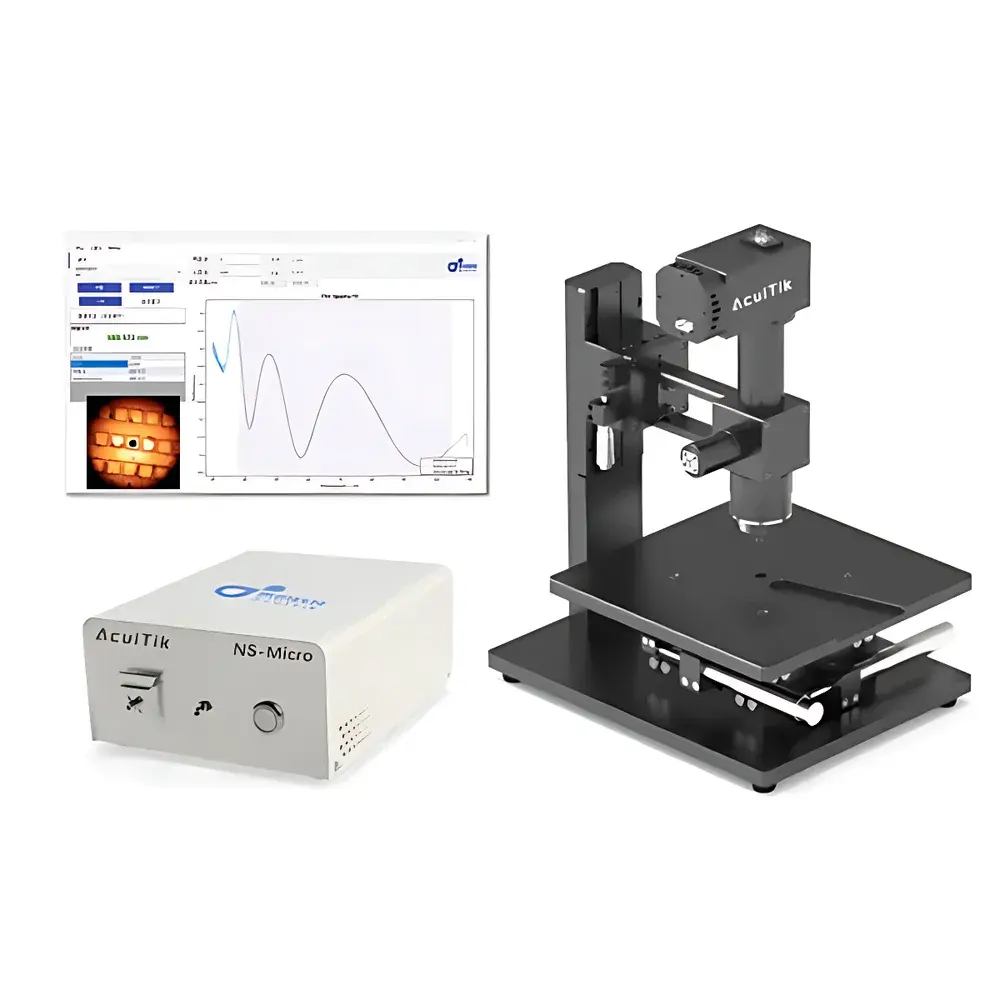
AcuiTik NanoSense NS-Micro Series Reflective Thin-Film Thickness Measurement System
| Brand | AcuiTik |
|---|---|
| Origin | Jiangsu, China |
| Manufacturer Type | OEM Manufacturer |
| Product Line | NS-Micro Series |
| Wavelength Range | 190–1000 nm |
| Thickness Measurement Range | 1–100 µm |
| Measurement Accuracy | ±1 nm or ±0.2% (whichever is greater) |
| Measurement Precision | 0.02 nm (1σ, 100 measurements on 500 nm SiO₂ reference) |
| Stability | 0.05 nm (2σ mean drift over 20 operational days) |
| Measurement Speed | <1 s per static point |
| Objective Options | 5×, 10×, 15×, 20×, 50×, 100× |
| Spot Size Range | 1–100 µm |
| Sample Diameter Capacity | 1 mm to ≥300 mm |
| Light Source | Deuterium + Tungsten-Halogen Lamp |
Overview
The AcuiTik NanoSense NS-Micro Series is a microscope-integrated, non-contact reflective thin-film thickness measurement system engineered for high-precision optical characterization of dielectric and semiconductor multilayer stacks. It operates on the principle of spectral reflectometry combined with white-light interferometry—capturing interference fringes generated by constructive and destructive interference between reflections from film interfaces. By analyzing the wavelength-dependent reflectance spectrum across the UV-Vis-NIR range (190–1000 nm), the system reconstructs layer thickness, refractive index, and extinction coefficient using rigorous thin-film optical modeling (e.g., transfer matrix method). Unlike conventional ellipsometers, the NS-Micro enables sub-micron spatial resolution via objective-coupled illumination, making it uniquely suited for localized metrology on patterned wafers, microfluidic devices, MEMS structures, and R&D-scale coated substrates where macroscopic averaging is inadequate.
Key Features
- Microscope-integrated architecture with modular spectral measurement head—enables seamless co-location of optical imaging and quantitative thickness analysis
- Adjustable measurement spot size (1–100 µm) selectable via motorized turret and objective lens interchange (5× to 100× magnification)
- Dual-source illumination: deuterium lamp (190–400 nm) and tungsten-halogen lamp (380–1000 nm) ensure continuous spectral coverage with stable radiometric output
- High-resolution manual XYZ translation stage (sub-micron repeatability) for precise positioning of measurement points on heterogeneous samples
- Integrated color CMOS camera providing real-time visual feedback with overlay of measurement crosshair and live spectral preview
- Calibration traceability to NIST-traceable Si/SiO₂ reference standards; accuracy validated per ISO 9001-compliant internal protocols
Sample Compatibility & Compliance
The NS-Micro supports transparent, semi-transparent, and weakly absorbing thin films—including SiO₂, Si₃N₄, Al₂O₃, ITO, polymer resists, and organic photovoltaic layers—on silicon, glass, sapphire, and metal substrates. It accommodates wafer diameters from 1 mm up to 300 mm (or larger with custom stage extension), accommodating both discrete coupons and full wafers. The system complies with key industry requirements for laboratory instrumentation: design and documentation align with GLP principles; data integrity safeguards include user-level access control, electronic signatures, and audit trail logging (aligned with FDA 21 CFR Part 11 readiness); measurement uncertainty budgets are documented per ISO/IEC 17025 guidance for accredited testing laboratories.
Software & Data Management
AcuiTik’s proprietary NanoSense Control Suite provides intuitive workflow-driven operation—from automated focus search and spectral acquisition to multi-layer model fitting and batch report generation. The software implements Levenberg-Marquardt nonlinear regression for rapid convergence on optical constants and thickness values. All raw spectra, fitted models, and metadata (timestamp, operator ID, instrument configuration) are stored in vendor-neutral HDF5 format. Export options include CSV, XML, and PDF reports compliant with internal QA templates. For integration into enterprise LIMS or MES environments, the system supports OPC UA and RESTful API interfaces, enabling automated data ingestion without manual export steps.
Applications
- Process development and qualification of ALD, PECVD, and spin-coated dielectric layers in semiconductor fabrication
- Thickness uniformity mapping across photomask blanks and EUV multilayer mirrors
- Quality assurance of anti-reflective, hard-coat, and barrier films on display cover glass and flexible OLED substrates
- R&D validation of nanostructured optical coatings (e.g., Bragg stacks, metamaterial absorbers)
- In-line process monitoring support via periodic sampling in pilot-line cleanroom environments
- Failure analysis of delamination or interfacial oxidation through comparative spectral residual analysis
FAQ
What film thickness ranges can the NS-Micro measure with different objectives?
With the 15× objective, the system measures films from 1 nm to 100 µm; the 100× objective supports high-resolution measurement down to 1 nm but is limited to ≤1 µm total thickness due to coherence length constraints.
Is calibration required before each measurement session?
No—factory calibration is retained across power cycles. However, daily verification using a certified Si/SiO₂ reference wafer is recommended per ISO 5725-2 precision guidelines.
Can the system analyze multilayer stacks with more than three layers?
Yes—the software supports up to 10-layer optical models with simultaneous fitting of thickness and complex refractive index (n + ik) for each layer.
Does the system meet regulatory requirements for pharmaceutical or medical device manufacturing?
While not classified as GMP-grade production equipment, its data management features—including electronic audit trails, role-based permissions, and 21 CFR Part 11–compatible signature workflows—support use in regulated R&D and QC labs under quality systems aligned with ICH Q5A and USP .
How is measurement uncertainty quantified and reported?
Uncertainty is calculated per GUM (JCGM 100:2008) methodology, incorporating contributions from spectral noise, stage repeatability, model parameter correlation, and reference standard uncertainty—fully documented in the exported measurement certificate.


