AcuiTik NS-30 White Light Interferometric Thin-Film Thickness Metrology System
| Brand | AcuiTik |
|---|---|
| Origin | Shanghai, China |
| Manufacturer Type | Direct Manufacturer |
| Model | NS-30 |
| Wavelength Range | 190–1700 nm (configurable UV/VIS/NIR variants) |
| Thickness Measurement Range | 1 nm – 250 µm |
| Accuracy | ±1 nm or ±0.2% (UV variant) |
| Precision | 0.02 nm (UV/VIS), 0.1 nm (NIR) |
| Stability | ≤0.05 nm (UV/VIS), ≤0.12 nm (NIR) |
| Spot Size | 1.5 mm |
| Single-Measurement Time | <1 s |
| Sample Diameter Capacity | 1 mm – 300+ mm |
| Automated Stage Travel | Up to 450 mm × 450 mm |
| Stress & Bow Measurement | Yes |
Overview
The AcuiTik NS-30 is a fully domesticated, benchtop white light interferometric (WLI) thin-film thickness metrology system engineered for high-precision, non-contact characterization of single- and multi-layer optical coatings on rigid and delicate substrates. Operating on the principle of spectral-domain white light interferometry, the NS-30 directs broadband collimated light vertically onto the sample surface; interference fringes generated at each dielectric interface are captured by a high-resolution spectrometer and resolved via proprietary inverse modeling algorithms. This enables simultaneous extraction of layer thickness, refractive index (n), extinction coefficient (k), reflectance, and—through curvature analysis—thin-film stress and substrate bow. Designed specifically for semiconductor process control, photovoltaic R&D, display manufacturing, and advanced optics development, the NS-30 delivers traceable, repeatable measurements across nanoscale (<1 nm) to microscale (250 µm) thickness regimes without physical contact or vacuum requirements.
Key Features
- Fully indigenous hardware and software architecture—100% domestically developed and controlled, compliant with national technology sovereignty requirements
- Modular optical engine supporting three interchangeable wavelength configurations: UV (190–1100 nm), VIS (380–1050 nm), and NIR (950–1700 nm), optimized for diverse material transparency windows
- Sub-nanometer static precision (0.02 nm) and long-term thermal-mechanical stability (≤0.05 nm drift over 8 hours)
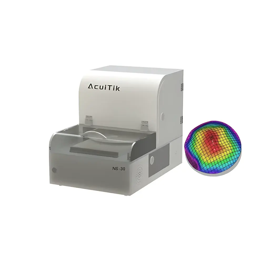
- Motorized XYZ stage with programmable positioning accuracy of ±0.5 µm, enabling automated grid-based mapping of wafers up to 300 mm in diameter
- Real-time stress and bow quantification derived from full-field topographic curvature fitting using ASTM F390-compliant methodology
- Patented PolarX analytical software with embedded optical dispersion models, multi-layer regression solvers, and recipe-driven measurement protocols
Sample Compatibility & Compliance
The NS-30 accommodates substrates ranging from 1 mm microchips to 300 mm silicon wafers, including glass, sapphire, fused silica, polymer films, and flexible OLED substrates. Its non-contact nature eliminates risk of surface deformation or contamination—critical for low-k dielectrics, photoresists, and soft organic layers. The system supports ISO/IEC 17025-aligned calibration traceability through NIST-traceable reference standards. Software audit trails, user access controls, electronic signatures, and data immutability features align with FDA 21 CFR Part 11 and GLP/GMP documentation requirements. All optical components comply with IEC 61000-6-3 EMC emission standards and CE safety directives.
Software & Data Management
PolarX—the proprietary analytical platform—integrates spectral acquisition, forward-modeling simulation, iterative layer parameter inversion, and spatial visualization in a unified GUI. It supports custom optical constant databases (Cauchy, Sellmeier, Tauc-Lorentz), multi-sample batch processing, and export of ASAM MCD-compliant metadata. Measurement reports include full spectral raw data, confidence intervals for fitted parameters, residual error maps, and statistical process control (SPC) charts. Data storage follows hierarchical file structures compliant with ISO 10360-7 for metrological instrument data integrity. Version-controlled software updates are delivered via secure OTA channels with SHA-256 checksum verification.
Applications
- Semiconductor front-end process monitoring: SiO₂, SiNₓ, HfO₂, Al₂O₃, and high-k gate stack thickness uniformity on 200/300 mm wafers
- Photovoltaic thin-film QC: CIGS, perovskite, and amorphous silicon layer thickness and compositional grading
- Optical coating R&D: Anti-reflective, dichroic, and HR mirror stack design validation and deposition feedback
- Display technology: ITO, AgNW, and conductive polymer film thickness and sheet resistance correlation studies
- MEMS and packaging: Low-stress passivation layer characterization and warpage-induced stress mapping
- Academic research: In-situ growth kinetics studies via time-resolved WLI under ambient or controlled environments
FAQ
Does the NS-30 require vacuum or inert atmosphere operation?
No—measurements are performed in ambient air; optional environmental chamber integration supports temperature- and humidity-controlled testing.
Can the system measure absorbing or opaque films?
Yes—within its configured spectral band, it resolves thickness of semi-transparent and weakly absorbing layers (e.g., TiN, Cr, NiCr) using amplitude-modulated fringe contrast analysis.
Is multi-layer stack analysis supported out-of-the-box?
Yes—PolarX includes pre-validated optical models for up to 7-layer stacks and allows user-defined dispersion relationships for novel materials.
How is calibration maintained across different wavelength modules?
Each module undergoes factory calibration against certified NIST SRM 2032 and SRM 1020a; field recalibration uses integrated reference mirrors with certified reflectance profiles.
What level of technical support and software maintenance is provided?
AcuiTik offers 3-year comprehensive support including remote diagnostics, firmware updates, application engineering consultation, and annual on-site performance verification per ISO/IEC 17025 clause 6.4.


