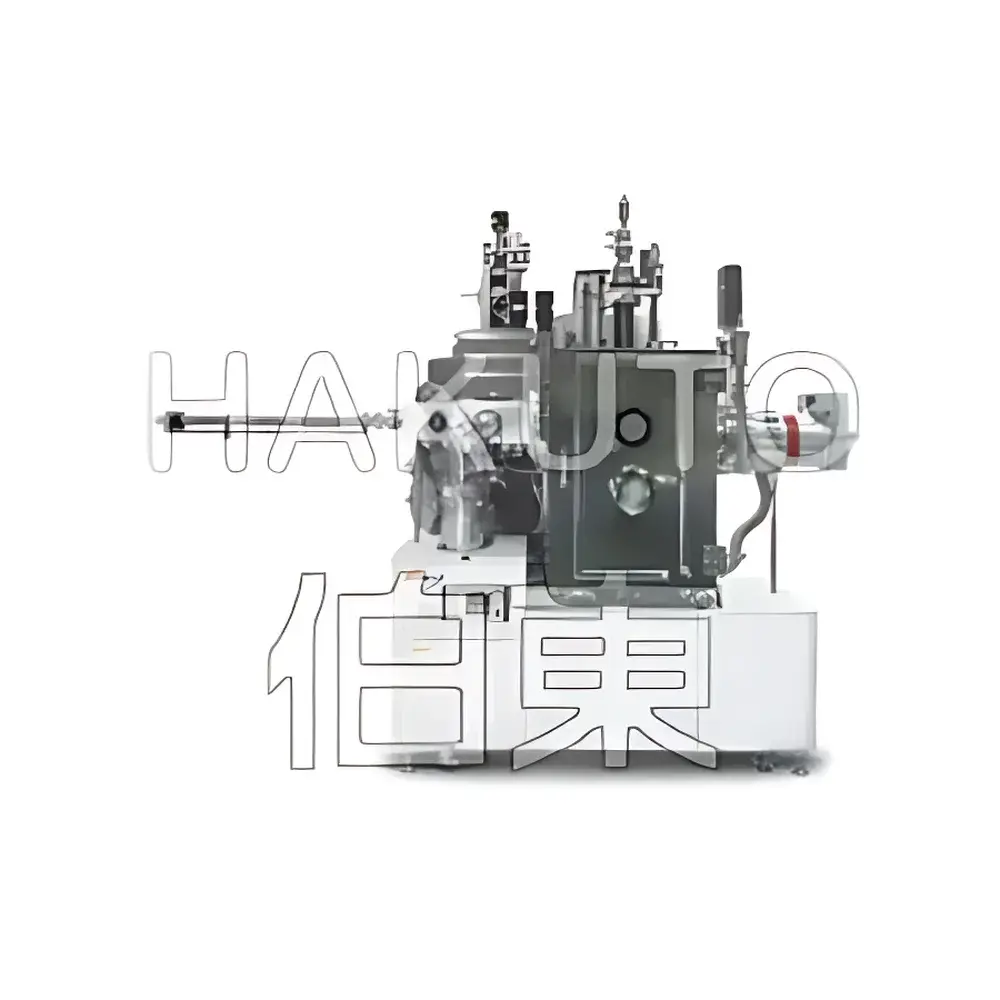
Syskey Lift-Off E-beam Evaporation System
| Brand | Syskey |
|---|---|
| Origin | Taiwan |
| Model | Lift-Off E-beam |
| Instrument Type | Electron Beam Evaporator |
| Application Domain | Microelectronics |
| Substrate Diameter | 12-inch (300 mm) |
| Maximum Substrate Temperature | 800 °C |
| Film Thickness Uniformity | ±3% |
| Base Pressure | 10⁻⁸ Torr |
| Cooling Options | Water-cooled or Liquid Nitrogen-cooled Substrate Holder (down to –70 °C) |
| Source Configuration | Multi-pocket e-beam gun (1/2/4/6 pockets) |
| Deposition Modes | Sequential or Co-evaporation |
Overview
The Syskey Lift-Off E-beam Evaporation System is a high-vacuum physical vapor deposition (PVD) platform engineered specifically for lift-off patterning in microelectronic device fabrication. Unlike conventional thermal evaporation, this system employs a focused electron beam to locally heat and vaporize source materials—enabling precise, contamination-controlled deposition of refractory metals (e.g., Pt, W, Mo, Ta), oxides, and ceramic compounds with melting points exceeding 3000 °C. The system operates on the fundamental principle of electron beam bombardment-induced sublimation within an ultra-high vacuum (UHV) environment, minimizing residual gas reactions and ensuring stoichiometric fidelity in multi-layer thin film stacks. Designed for process reproducibility and integration into cleanroom-compatible workflows, it supports both single-material deposition and synchronized co-evaporation across up to six independently controlled e-beam sources.
Key Features
- Ultra-high vacuum chamber with base pressure ≤1×10⁻⁸ Torr, achieved via turbomolecular pumping backed by dry scroll or cryogenic roughing—ensuring low hydrocarbon background and minimal oxide formation during metal deposition.
- Modular multi-pocket e-beam gun assembly (configurable for 1, 2, 4, or 6 crucibles), each pocket thermally isolated and individually controllable for sequential or simultaneous material evaporation.
- Substrate stage with dual-mode temperature control: resistive heating up to +800 °C and active cooling via liquid nitrogen (–70 °C) or recirculating chiller—critical for stress management and interfacial adhesion in lift-off-compatible films.
- High-precision thickness monitoring using quartz crystal microbalance (QCM) with real-time rate feedback, enabling closed-loop control of deposition rates and achieving ±3% thickness uniformity across 12-inch (300 mm) wafers.
- Robust anti-contamination architecture: water-cooled e-beam source housing, directional shielding, and crucible liners minimize cross-talk between dissimilar materials during multi-source operation.
- Customizable chamber geometry—diameters up to 650 mm—to accommodate large-area substrates or auxiliary modules such as load-lock interfaces, robotic transfer arms, or inert-atmosphere glovebox integration.
Sample Compatibility & Compliance
The system accommodates standard semiconductor substrates including Si, GaAs, sapphire, fused silica, and flexible polymer foils—compatible with photolithographically defined lift-off resists (e.g., LOR series, PMMA bilayers). All vacuum components conform to ASTM F2783 (Standard Practice for Vacuum Chamber Leak Testing) and ISO 10110-7 (optical surface cleanliness specifications). The chamber design supports GLP/GMP-aligned documentation protocols; optional audit-trail-enabled software logs all critical process parameters—including source current, substrate temperature, chamber pressure, deposition rate, and time-stamped event markers—in accordance with FDA 21 CFR Part 11 requirements for regulated R&D environments.
Software & Data Management
Integrated control software provides deterministic recipe management with support for up to 99 programmable deposition steps per run. Each step defines e-beam power ramp profiles, shutter sequencing, QCM setpoints, and thermal stage trajectories. Process data—including real-time thickness curves, pressure transients, and source emission stability—are logged in HDF5 format for traceability and post-run analysis. Export options include CSV, MATLAB .mat, and industry-standard SECS/GEM protocol support for factory automation integration. Remote diagnostics and firmware updates are performed over secure TLS-encrypted Ethernet connections, with role-based access control (RBAC) compliant with NIST SP 800-53 controls.
Applications
- Lift-off fabrication of high-aspect-ratio metallic interconnects (Au, Al, Ti/Pt, NiCr) without ion-beam damage or undercutting issues common in wet etching.
- Deposition of diffusion barriers (e.g., TiN, TaN) and seed layers for subsequent electroplating in advanced packaging and MEMS processes.
- Growth of optoelectronic thin films—including ITO, ZnO, and perovskite precursors—where stoichiometry preservation requires non-thermal, low-background evaporation.
- Research-scale synthesis of heterostructured multilayers (e.g., magnetic tunnel junctions, superconducting NbN/TiN stacks) requiring atomic-level interface control and minimal interdiffusion.
- In-situ calibration of reference standards for XRD, XPS, and ellipsometry—leveraging the system’s repeatability and certified thickness accuracy.
FAQ
What vacuum level is required for high-purity metal film deposition?
A base pressure ≤1×10⁻⁸ Torr is essential to suppress oxidation, nitridation, and carbon incorporation—particularly for reactive metals such as Ti, Cr, and Al.
Can the system deposit insulating materials like Al₂O₃ or SiO₂?
Yes—using conductive crucible liners (e.g., graphite or tantalum) and optimized e-beam focusing, dielectric oxides can be evaporated with controlled oxygen partial pressure via optional MFC-controlled O₂ inlet.
Is the system compatible with automated wafer handling?
Standard configurations include CF-100 or ISO-K200 flanges for integration with load-lock chambers, cluster tools, and SECS/GEM-compliant robotic transfer systems.
How is film uniformity validated across 12-inch substrates?
Uniformity is verified using calibrated profilometry (Dektak) and spectrophotometric mapping (UV-Vis/NIR) on witness wafers, with SOPs aligned to SEMI F20-0212 standards.
Does the system support in-situ monitoring beyond QCM?
Optional add-ons include reflection high-energy electron diffraction (RHEED), optical emission spectroscopy (OES), and laser interferometric thickness monitoring for real-time growth mode analysis.
Related Products


