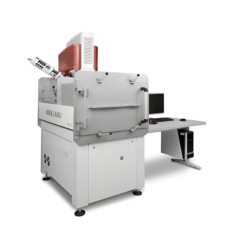
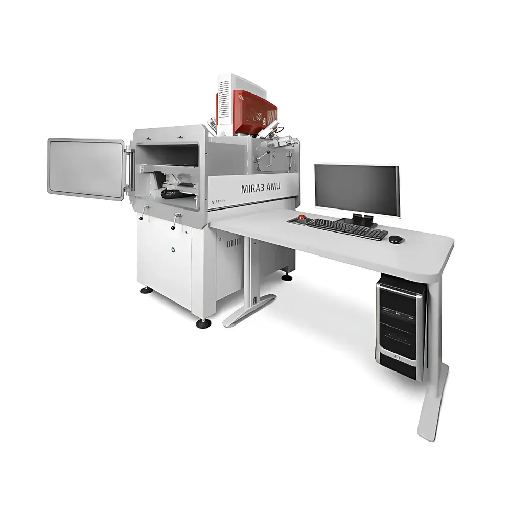
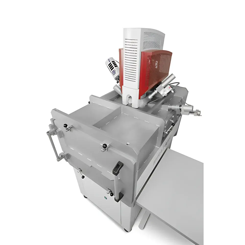
TESCAN MIRA AMU Customized Large-Chamber Field-Emission Scanning Electron Microscope
| Brand | TESCAN |
|---|---|
| Origin | Czech Republic |
| Manufacturer | TESCAN ORSAY HOLDING a.s. |
| Type | Floor-Standing SEM |
| Electron Source | Schottky Field-Emission Gun |
| Secondary Electron Resolution | 1.0 nm @ 30 kV |
| Backscattered Electron Resolution | 2.0 nm @ 30 kV |
| Magnification Range | ×2 to ×1,000,000 |
| Accelerating Voltage | 50 V (decelerated mode) to 30 kV |
| Chamber Configuration | AMU (Advanced Macro-Utility) Ultra-Large Specimen Chamber |
| Compliance | CE, ISO 9001, IEC 61000-6-3/6-4 |
Overview
The TESCAN MIRA AMU is a floor-standing field-emission scanning electron microscope engineered for high-resolution imaging, compositional analysis, and structural characterization of macro- to micro-scale specimens under demanding research and industrial conditions. Leveraging a high-brightness Schottky thermionic field-emission electron source, the system delivers exceptional signal-to-noise ratio, stable beam current up to 200 nA, and sub-nanometer secondary electron resolution at 30 kV — enabling reliable imaging and analytical performance across voltage ranges from 50 V (via deceleration optics) to 30 kV. Its proprietary Wide Field Optics™ three-lens electron optical column provides extended depth of field, large field-of-view acquisition, and seamless switching between low- and high-magnification modes without mechanical aperture changes. Real-time In-Flight Beam Tracing™ software enables dynamic simulation and optimization of beam trajectories during operation, supporting reproducible alignment and quantitative metrology workflows.
Key Features
- AMU ultra-large specimen chamber accommodating samples up to Ø350 mm × H300 mm — ideal for in situ mechanical testing, large-area geological sections, turbine blades, or full PCB assemblies
- Schottky field-emission gun with auto-tuning and long-term emission stability (>1,000 hours between cleanings)
- Integrated In-Beam SE detector for ultra-high-resolution surface imaging at low kV, minimizing charging effects on insulating materials
- Dynamic and static image distortion correction algorithms synchronized with scan generator timing for geometric fidelity at high magnifications
- Motorized multi-axis eucentric stage with ±70° tilt, 360° rotation, and 100 mm X-Y travel — fully programmable via Python API
- Automated vacuum interlock, column alignment, stigmator tuning, and focus routines reduce operator dependency and increase throughput
- Modular detector architecture supporting simultaneous acquisition from multiple signals: SE, BSE, EDS, EBSD, CL, and STEM-in-SEM
Sample Compatibility & Compliance
The MIRA AMU supports diverse sample geometries — from bulk metallic alloys and ceramic composites to hydrated biological tissues (with optional low-vacuum or ESEM mode), semiconductor wafers, and additive-manufactured components. Its large-chamber design eliminates the need for sectioning oversized specimens, preserving contextual integrity for failure analysis and process validation. The system complies with ISO 16700 (SEM measurement uncertainty), ASTM E1558 (EBSD sample preparation), and IEC 61000 electromagnetic compatibility standards. For regulated environments, optional FDA 21 CFR Part 11-compliant audit trail logging, electronic signatures, and role-based access control (RBAC) are available through the UnifiedPlatform™ software suite — supporting GLP/GMP-aligned quality assurance protocols.
Software & Data Management
Controlled by TESCAN’s UnifiedPlatform™ — a modular, Python-extendable software environment — the MIRA AMU offers native support for automated scripting, batch acquisition, and integrated data pipelines. Core modules include SmartAlign™ (auto-alignment), SmartScan™ (adaptive dwell time optimization), and 3D Surface Reconstruction (stereo-SEM). Image metadata is embedded per DICOM-SR and TIFF/OME-BigData standards. Raw data export supports HDF5, EMF, and MRC formats for third-party processing (e.g., DigitalMicrograph, MATLAB, or TomoJ). Network-enabled remote diagnostics, live collaborative session sharing, and centralized license management facilitate multi-site deployment and IT-integrated lab infrastructure.
Applications
- Materials science: Grain boundary mapping via EBSD, phase identification with WDS, porosity quantification in battery electrodes or catalyst substrates
- Geosciences: Petrographic analysis of drill cores, microfossil morphology, and pore-network modeling in shale reservoirs
- Electronics: Cross-sectional inspection of TSVs, solder joint integrity assessment, and contamination tracing on 300 mm wafers
- Life sciences: Correlative light-electron microscopy (CLEM) sample navigation, freeze-fracture replica imaging, and serial block-face SEM (SBF-SEM) workflow integration
- Forensics & failure analysis: Fractography of fractured turbine disks, gunshot residue particle classification, and counterfeit component authentication
FAQ
What vacuum configurations does the MIRA AMU support?
It operates in high vacuum (HV) mode (<1×10⁻⁵ Pa) for maximum resolution and analytical sensitivity; optional variable pressure (VP) and low-vacuum (LV) modes enable imaging of non-conductive, hydrated, or outgassing samples without sputter coating.
Is the system compatible with third-party EDS/WDS detectors?
Yes — the MIRA AMU features standardized detector ports (IEEE 1394, USB3, and analog TTL) and provides SDK-level integration support for Oxford Instruments, EDAX, and Bruker hardware.
Can the AMU chamber be retrofitted with in-situ stages?
Yes — the chamber includes dedicated feedthroughs and clearance for heating, cooling, tensile, and electrochemical in-situ stages from Kammrath & Weiss, DENSsolutions, and Protochips.
How is beam alignment maintained during long-term unattended operation?
Auto-alignment sequences run periodically using reference grid patterns and beam-induced current feedback; drift compensation is applied in real time via stage position correction and scan-frame registration.
Does the system support automated particle analysis across heterogeneous surfaces?
Yes — ParticleMetric™ module enables statistically robust size, shape, and composition classification across stitched mosaics >100 mm², with customizable thresholds and ISO 13322-2 compliant reporting templates.


