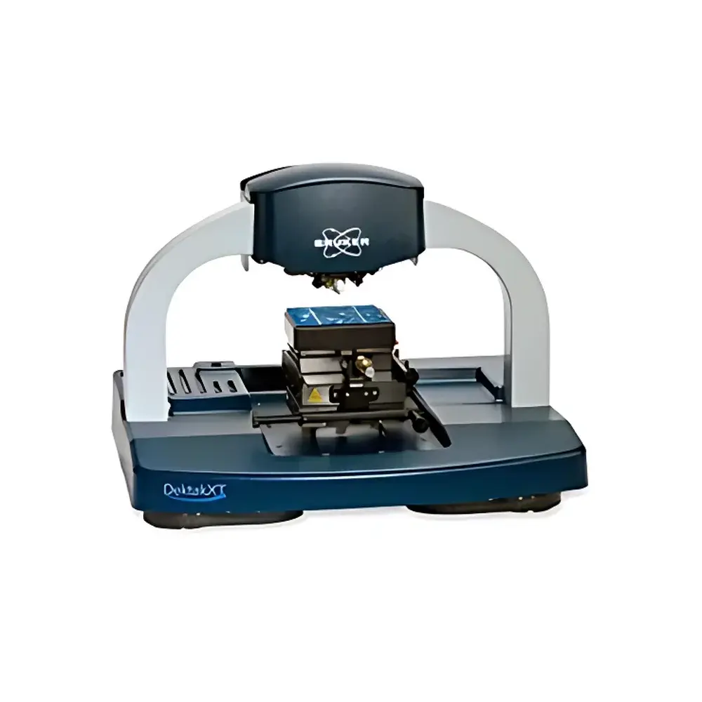
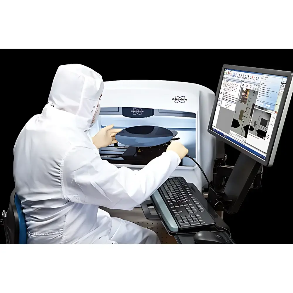
Bruker Dektak XTL Stylus Profilometer System
| Brand | Bruker |
|---|---|
| Origin | USA |
| Manufacturer Type | Authorized Distributor |
| Origin Category | Imported |
| Model | Dektak XTL |
| Pricing | Available Upon Request |
| Measurement Principle | Capacitive Transduction |
| Measurement Capability | 2D Surface Topography (Optional 3D Reconstruction) |
| Accuracy | ±0.5% of measured step height |
| Probe Tip Radius | 50 nm – 25 µm |
| Normal Force Range | 0.3–15 mg |
| Maximum Scan Length | 55 µm |
| Step Height Repeatability | 5 Å (1σ, on 1 µm step) |
| Vertical Resolution | Up to 1 Å (within 6.55 µm vertical range) |
| Maximum Sample Size | 300 mm diameter |
Overview
The Bruker Dektak XTL Stylus Profilometer is a high-precision, production-grade surface metrology instrument engineered for quantitative step height, roughness, and thin-film thickness characterization across semiconductor wafers, flat-panel displays, advanced packaging substrates, and flexible electronics. Based on proven capacitive transduction technology, the system measures vertical displacement with sub-angstrom resolution by tracking the deflection of a mechanically scanned diamond or silicon carbide stylus in contact with the sample surface. Unlike optical interferometric or confocal methods, stylus profilometry provides direct traceable measurement of topographic features—including steep sidewalls, buried interfaces, and low-contrast organic layers—without reliance on optical reflectivity or coherence conditions. The Dektak XTL integrates a rigid granite base, active pneumatic isolation, and an interlocked fully enclosed chamber to ensure mechanical stability and environmental immunity—critical for high-yield manufacturing environments operating under ISO Class 7 cleanroom conditions or GLP-compliant laboratories.
Key Features
- Dual high-resolution coaxial cameras with real-time video overlay enable intuitive point-and-click navigation, automatic leveling via two-point selection, and rapid scan path definition directly from live imagery.
- Motorized 300 mm encoded XY stage with full 360° continuous rotation supports unlimited positional programming and multi-site measurement across large-area substrates up to 300 mm in diameter.
- Vision64 software platform—fully compatible with Bruker’s optical profiler product line—delivers unified workflow management for 2D line profiling, 3D surface reconstruction, and automated feature extraction using built-in pattern recognition algorithms.
- Integrated VisionMicroform module extends capability to curvature radius, spherical deviation, and form error analysis of non-planar surfaces such as lens molds or micro-optics.
- Probe force control (0.3–15 mg) and tip radius selection (50 nm–25 µm) allow optimization for soft polymers, brittle oxides, or ultra-thin metal films while maintaining <5 Å repeatability on 1 µm steps (1σ).
- All systems ship with perpetual Vision64 software licenses validated for Windows 7/10/11, supporting local desktop analysis, report generation, and database archiving of metadata, user-defined prompts, and calibration logs.
Sample Compatibility & Compliance
The Dektak XTL accommodates rigid and semi-rigid substrates up to 300 mm in diameter and 50 mm in thickness—including silicon wafers, fused silica masks, glass panels (G2–G8), copper-clad PCBs, and PET-based flexible OLED substrates. Its closed-chamber architecture meets ANSI/ISO 14644-1 Class 7 particulate requirements when installed in controlled environments. Data acquisition and reporting workflows support audit-ready documentation per FDA 21 CFR Part 11 (electronic signatures, audit trails, user access controls) and are routinely validated for GMP manufacturing processes in semiconductor foundries and display fabrication facilities. Calibration traceability follows NIST SRM standards (e.g., NIST SRM 2150a for step height), and measurement uncertainty budgets comply with ISO/IEC 17025:2017 requirements for accredited testing laboratories.
Software & Data Management
Vision64 serves as the central analytical engine—providing scriptable automation, batch processing, and customizable reporting templates compliant with internal SOPs and external regulatory submissions. Raw profilometry data (Z-height vs. X-position) is stored in vendor-neutral ASCII or Bruker-native .pro format, enabling third-party integration with MATLAB, Python (via Bruker SDK), or enterprise MES/QMS platforms. Each measurement record includes embedded metadata: operator ID, timestamp, probe parameters, environmental log (temperature/humidity if monitored), and calibration certificate reference. Optional database modules support SQL-based querying across thousands of measurements, facilitating statistical process control (SPC) charting, trend analysis, and root-cause investigation of process drift.
Applications
- Semiconductor Process Control: Etch rate uniformity, CMP dishing/erosion, photoresist thickness, hard mask integrity, and gate stack step coverage on 200–300 mm wafers.
- Flat Panel Display Manufacturing: ITO trace height on touch sensors, OLED pixel bank height, color filter spacer dimensions, and encapsulation layer conformity on Gen 4–Gen 8 glass substrates.
- Advanced Packaging: Redistribution layer (RDL) topography, solder bump coplanarity, underfill fillet geometry, and through-silicon via (TSV) depth profiling.
- Flexible Electronics R&D: Thickness mapping of PEDOT:PSS, PVK, or perovskite layers on PET/PEN substrates; edge definition analysis of laser-scribed electrodes in AMOLED backplanes.
- Optical Component Metrology: Radius-of-curvature verification of molded microlenses, wedge angle quantification in beam splitters, and form error assessment of IR window coatings.
FAQ
What is the maximum vertical range supported in high-resolution mode?
The Dektak XTL achieves 1 Å vertical resolution within a 6.55 µm full-scale range. Extended ranges up to 1.2 mm are available via auto-ranging, with corresponding resolution trade-offs per ISO 25178-6 guidelines.
Can the system measure transparent or low-reflectivity films?
Yes—stylus profilometry is insensitive to optical properties. It reliably measures polymer resists, SiO₂ anti-reflective coatings, and carbon-based barrier layers where optical methods fail due to phase ambiguity or poor signal-to-noise ratio.
Is Vision64 compatible with Bruker’s optical profilers?
Yes—Vision64 uses a common API and file structure across Bruker’s entire surface metrology portfolio, enabling seamless cross-platform data comparison and unified reporting workflows.
How is probe wear monitored and compensated?
Vision64 includes automated tip wear diagnostics using reference step standards and real-time force feedback logging. Users may apply tip-shape correction models during post-processing per ISO 25178-2 Annex B recommendations.
Does the system support automated pass/fail decision logic?
Yes—customizable pass/fail thresholds can be defined per feature type (e.g., “step height > 95 nm AND < 105 nm”) and exported to factory SCADA systems via OPC UA or Modbus TCP protocols.