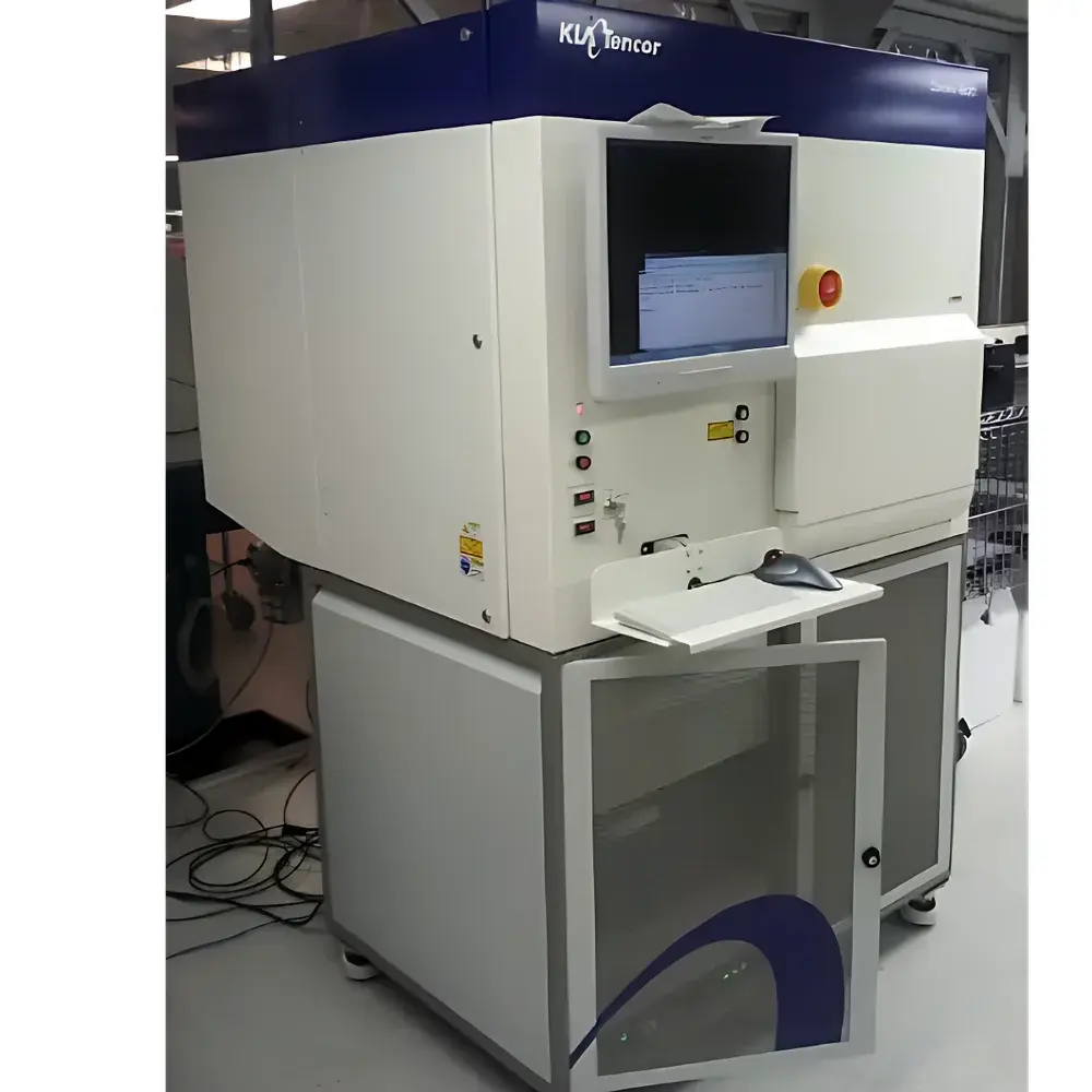
KLA Candela 8420 Optical Surface Defect Inspection System
| Brand | KLA |
|---|---|
| Origin | Singapore |
| Manufacturer Type | Authorized Distributor |
| Origin Category | Imported |
| Model | Candela 8420 |
| Pricing | Available Upon Request |
| Instrument Category | Optical Non-Patterned Wafer Defect Inspection System |
| Primary Application | Surface Defect Detection on Unpatterned Wafers |
| Wafer Diameter | 2–8 inches |
| Throughput | 30 WPH |
| Resolution | 83 nm |
Overview
The KLA Candela 8420 is a high-sensitivity, non-patterned wafer surface inspection system engineered for rapid, high-resolution detection of sub-100 nm defects on bare and semi-transparent substrates. Utilizing advanced dark-field laser scattering (DFLS) optics combined with multi-angle illumination and polarization-controlled detection, the system identifies particles, pits, bumps, scratches, haze, and localized contamination across diverse material platforms—including silicon, fused silica, sapphire (single- and double-side polished), lithium tantalate (LiTaO₃), and other advanced piezoelectric or optical substrates. Its design adheres to semiconductor front-end manufacturing requirements where early defect excision—prior to film deposition or lithography—is critical to yield ramp and process control. The Candela 8420 operates without reliance on reference die or pattern matching, making it inherently suitable for monitor wafers, epitaxial wafers, reclaimed wafers, and pre-process qualification lots.
Key Features
- Sub-100 nm sensitivity: Achieves consistent detection of 83 nm polystyrene latex (PSL) equivalent particles under standard operating conditions.
- Multi-material compatibility: Optimized optical path and detector gain calibration support opaque (Si), semi-transparent (sapphire), and fully transparent (glass, LiTaO₃) substrates without hardware reconfiguration.
- High-throughput architecture: Delivers up to 30 wafers per hour (WPH) at full resolution for 8-inch wafers, with automated load/unload integration via SECS/GEM-compliant interfaces.
- Surface haze mapping capability: Generates quantitative, pixel-resolved haze intensity profiles using integrated broadband reflectance normalization—enabling correlation between scatter signatures and bulk/subsurface inhomogeneity.
- Robust environmental control: Integrated temperature stabilization and vibration isolation ensure measurement repeatability across shifts and facility locations.
- Modular upgrade path: Supports optional add-ons including UV-enhanced illumination, backside inspection mode, and automated defect review linkage with KLA’s eDR™ platform.
Sample Compatibility & Compliance
The Candela 8420 accommodates unpatterned wafers ranging from 50 mm (2″) to 200 mm (8″) in diameter, including edge-excluded and notch-aligned formats. It complies with SEMI standards for mechanical interface (SEMI E1, E2, E3, E39), communications (SEMI E30, E40, E57), and data formatting (SEMI E142). All defect classification outputs are structured in SEMI E142-compliant XML schema and support traceability per ISO 9001 and IATF 16949 quality management systems. For regulated environments, audit trail logging, user access controls, and electronic signature support align with FDA 21 CFR Part 11 requirements when deployed with KLA’s certified software stack (Candela OS v5.2+).
Software & Data Management
The system runs on KLA’s proprietary Candela OS, featuring real-time scatter event clustering, hierarchical defect binning (based on size, morphology, and spatial distribution), and statistical process control (SPC) dashboarding. Raw scatter maps and classified defect lists export directly to KLA’s Panorama™ analytics suite for cross-tool correlation, excursion root-cause analysis, and yield impact modeling. All data—including instrument configuration logs, calibration records, and operator actions—are stored with immutable timestamps and SHA-256 hashing to satisfy GLP/GMP documentation integrity requirements. Integration with factory MES via SECS/GEM ensures automatic job dispatch and result feedback without manual intervention.
Applications
- Front-end process monitoring: Detection of polishing-induced scratches, CMP residue, and post-clean particle adders on prime and epitaxial Si wafers.
- Advanced substrate qualification: Inspection of sapphire and LiTaO₃ blanks for RF filter and SAW device fabrication, where subsurface voids and crystallographic slip lines directly impact device reliability.
- Haze-driven yield loss analysis: Quantitative correlation of haze map gradients with subsequent thin-film adhesion failures or lithographic CD variation.
- Recycled wafer screening: Rapid assessment of reclaimed wafers for residual metal contamination and micro-roughness prior to re-use in low-criticality layers.
- Materials R&D: Defect baseline establishment for novel substrates such as GaN-on-Si, SiC, and 2D material transfer carriers.
FAQ
What wafer materials can the Candela 8420 inspect without modification?
Silicon, fused quartz, single- and double-side polished sapphire, lithium tantalate, lithium niobate, and borosilicate glass—all supported natively via auto-material recognition and dynamic gain adjustment.
Does the system support automated defect review or classification?
It provides primary classification (particle, pit, bump, haze cluster) and exports coordinates and scatter signatures for downstream review; full automated classification requires integration with KLA’s eDR™ or third-party AI-based review tools.
Is the 83 nm resolution specified for all substrate types?
The 83 nm PSL-equivalent sensitivity is validated on silicon and fused silica; for highly transparent or low-scatter materials (e.g., LiTaO₃), effective resolution may vary ±10% depending on surface roughness and ambient stray light control.
Can the Candela 8420 be integrated into an automated fab environment?
Yes—it supports full SECS/GEM communication, SMIF/FOUP handling interfaces, and recipe-based operation compatible with AMHS and MES-level scheduling protocols.
How is calibration maintained across shifts?
Daily automated verification using NIST-traceable PSL standards is enforced via built-in calibration wafers; drift correction algorithms update detector gain and laser power parameters in real time during inspection runs.


