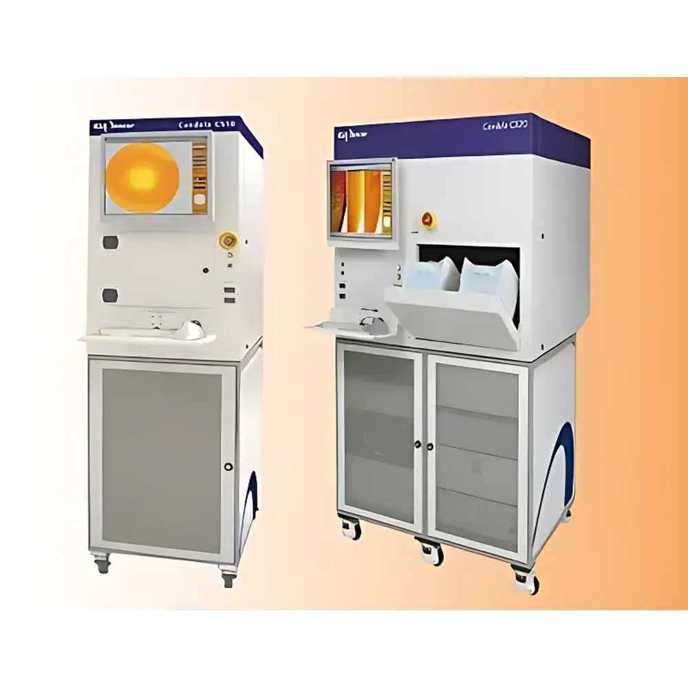
KLA-Tencor Candela CS10/CS20 Surface Defect Inspection System
| Brand | KLA |
|---|---|
| Origin | USA |
| Model | CS10 / CS20 |
| Detection Sensitivity | 80 nm particles |
| Sample Size Support | 2–8 inch wafers (standard), customizable fixtures |
| Operation Modes | Manual (CS10) / Automated Transport (CS20) |
| Optical Channels | 4-channel detection (scattered light, reflected light, phase shift, Z-height) |
| Environmental Class | ISO Class 4 (10 cleanroom equivalent) |
| Compliance | Designed for semiconductor fab environments |
| Software | Integrated defect classification, statistical distribution mapping, root-cause traceability, and automated pass/fail reporting |
Overview
The KLA-Tencor Candela CS10/CS20 Surface Defect Inspection System is a high-precision, non-contact optical inspection platform engineered for semiconductor manufacturing environments. It employs multi-channel laser scanning technology—based on angular-resolved light scattering and interferometric height profiling—to detect, localize, and classify surface anomalies on bare and patterned wafers, compound semiconductor substrates (e.g., GaAs, SiC, GaN), and optically transparent materials such as quartz, sapphire, and fused silica. Unlike single-mode imaging tools, the CS10/CS20 acquires synchronized signals across four independent optical channels: scattered intensity (for particle detection), specular reflectance (for macro-defects and film interference), phase-shift contrast (for sub-surface and low-contrast features), and Z-height topography (for pit/scratch depth and step-height quantification). This multi-modal acquisition enables robust differentiation between physical defects (e.g., particles ≥80 nm), process-induced residues (e.g., watermarks, etch residues), mechanical damage (scratches, digs), and topographic variations (roughness, bow, warp)—all without sample preparation or vacuum requirements.
Key Features
- Multi-wavelength dual-laser illumination system optimized for sensitivity across dielectric and conductive surfaces
- Real-time, full-wafer scanning at throughput rates up to 25 wafers/hour (CS20 with auto-loader)
- Sub-100 nm particle detection capability validated per SEMI MF1719 and ISO 14644-1 Annex B protocols
- Integrated Z-channel interferometry enabling quantitative depth profiling of pits and scratches with ±2 nm repeatability
- Modular fixture design supporting 2-inch to 8-inch round and square substrates; custom carriers available for non-standard geometries
- Onboard ISO Class 4 (10) clean environment maintained via HEPA-filtered recirculation and positive-pressure enclosure—eliminating internal contamination drift during extended operation
- Automated defect binning using supervised machine learning classifiers trained on KLA’s proprietary defect library (including >200 reference signatures)
Sample Compatibility & Compliance
The CS10/CS20 accommodates bare silicon, SOI, SiGe, III-V compound wafers, glass substrates, and polished ceramic carriers used in advanced packaging. Its optical architecture supports both reflective and transmissive modes, making it suitable for frontside, backside, and through-transmission inspection of thin-film-coated or bonded wafers. The system complies with industry-standard metrology frameworks: data integrity meets FDA 21 CFR Part 11 requirements via audit-trail-enabled software logging; environmental control aligns with ISO 14644-1 Class 4 specifications; and measurement traceability follows NIST-traceable calibration protocols per SEMI E137. All hardware and firmware are qualified for integration into 24/7 fab automation systems (SECS/GEM compliant) and support GLP/GMP documentation workflows.
Software & Data Management
The integrated Candela Inspector Suite provides a unified interface for recipe management, real-time defect review, statistical process control (SPC), and cross-tool correlation. Each detected defect is stored with synchronized 4-channel image snapshots, spatial coordinates, size metrics (area, diameter, height), and classification confidence scores. Raw data export supports HDF5 and CSV formats for external analysis in MATLAB, Python (NumPy/Pandas), or JMP. The software includes built-in SPC dashboards with Cpk, DPU, and yield trend analysis; automated report generation (PDF/HTML) with configurable pass/fail thresholds per defect type and location zone; and secure role-based access control (RBAC) aligned with ISO/IEC 27001 principles. Audit trails record all user actions—including parameter edits, classification overrides, and report exports—with immutable timestamps.
Applications
- Front-end process monitoring: Particle monitoring post-clean, post-etch, and post-CMP; residue detection after lithography and stripping
- Back-end and packaging: Wafer-level inspection pre-dicing; bump and RDL defect screening; substrate cleanliness verification for fan-out wafer-level packaging (FOWLP)
- Material qualification: Incoming wafer acceptance testing for micro-roughness, flatness (TTV, BOW, WARP), and film uniformity (via reflectance modulation analysis)
- Failure analysis support: Correlation of defect maps with SEM/FIB cross-sections and EDX composition data to isolate root causes (e.g., slurry agglomeration vs. tool-induced scratching)
- Process development: Quantitative feedback for optimizing CMP slurries, cleaning chemistries, and spin-rinse-dry parameters
FAQ
What wafer sizes does the CS10/CS20 support out of the box?
Standard configurations include motorized chucks for 2-inch, 4-inch, 6-inch, and 8-inch wafers. Custom carriers for 12-inch wafers and non-circular substrates (e.g., rectangular GaN templates) are available under engineering services.
Can the system distinguish between particles and surface scratches?
Yes—through combined analysis of scattered-light intensity profile, phase-contrast morphology, and Z-height discontinuity, the software classifies particles, linear scratches, pits, and raised features with >95% accuracy in production settings.
Is the system compatible with automated material handling systems (AMHS)?
The CS20 model includes SECS/GEM interface compliance and FOUP/SMIF port options for seamless integration into factory automation networks.
How is calibration maintained over time?
The system performs daily self-calibration using on-board NIST-traceable reference standards; annual verification is performed by KLA-certified field service engineers following SEMI E137 procedures.
Does the software support multi-site data aggregation?
Yes—the Candela Inspector Suite supports centralized database deployment (Microsoft SQL Server or Oracle) with secure TLS-encrypted remote access for global fab network analytics.


