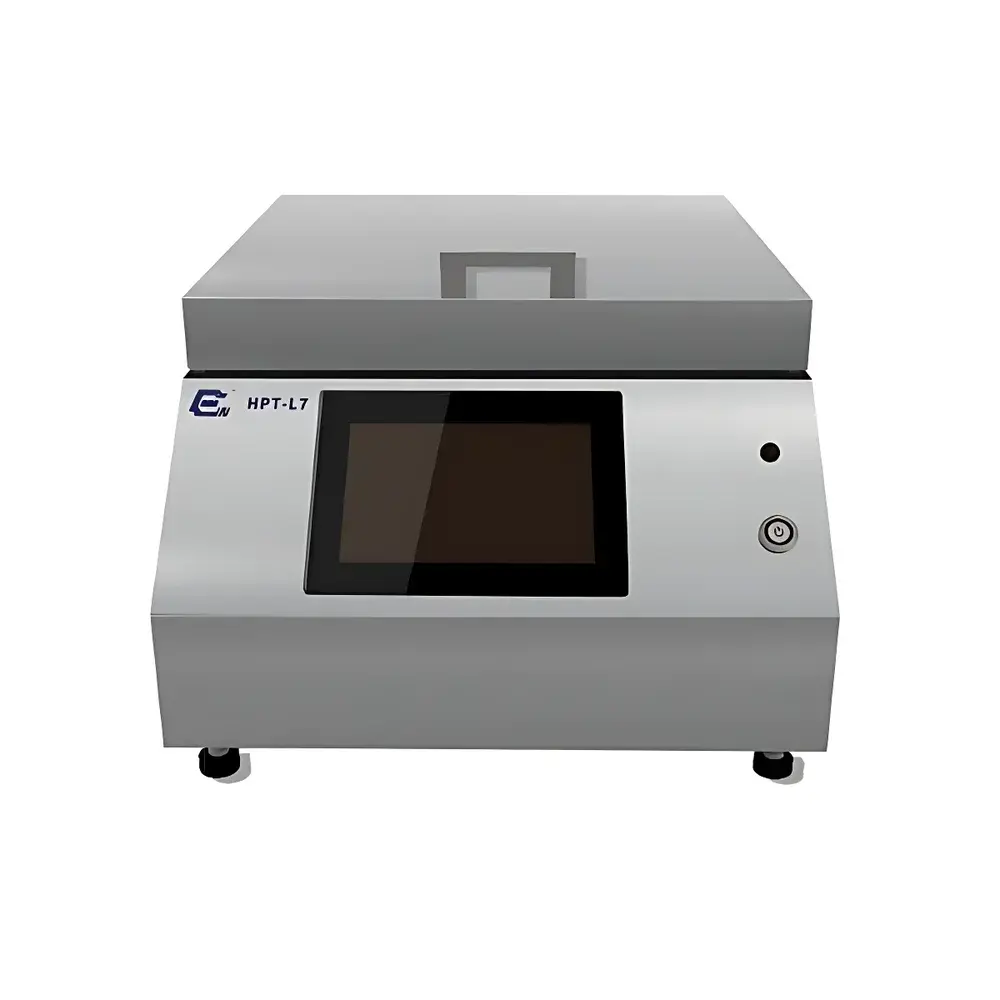
HPT-L7 High-Precision Hot Plate System by EWIN-TECH
| Brand | EWIN-TECH |
|---|---|
| Origin | Shanghai, China |
| Manufacturer Type | OEM/ODM Manufacturer |
| Country of Origin | China |
| Model | HPT-L7 |
| Pricing | Upon Request |
Overview
The HPT-L7 High-Precision Hot Plate System is an engineered thermal processing platform designed specifically for semiconductor R&D, micro/nano-fabrication, and optoelectronic device development. It operates on the principle of conductive heat transfer via a precisely regulated aluminum heating surface, optimized for photolithography-related thermal steps—including pre-bake (soft bake) and post-exposure bake (PEB)—where temperature accuracy, spatial uniformity, and contamination control are critical to resist performance and pattern fidelity. Unlike conventional convection ovens or infrared heaters, the HPT-L7 delivers rapid thermal response and minimal thermal lag through direct contact (or controlled non-contact) with substrates, making it suitable for wafer-level processing in Class 100–Class 1000 cleanroom environments.
Key Features
- High-Fidelity Thermal Control: Temperature range from ambient to 250 °C with 0.1 °C setpoint resolution and ±2% spatial uniformity across the heating surface—validated per ASTM E220 and ISO/IEC 17025 traceable calibration protocols.
- Non-Contact Bake Mode: Motorized, height-adjustable quartz or ceramic lift pins (0–30 mm travel) enable precise gap control between substrate and hot plate surface, minimizing particle generation and mechanical stress on fragile or ultra-thin wafers (e.g., <100 µm Si, flexible PI substrates).
- Multi-Step Programmable Profile: Supports up to 12 independent temperature/time segments per recipe, enabling complex ramp-hold-cool sequences required for advanced photoresist systems (e.g., chemically amplified resists), low-k dielectric curing, or metal oxide semiconductor annealing.
- Industrial-Grade Human-Machine Interface: 7-inch TFT color touchscreen with intuitive GUI, integrated PLC-based motion and thermal logic, real-time parameter logging, and recipe management with user-level access control (admin/operator modes).
- Cleanroom-Optimized Construction: Anodized aluminum heating plate (Type II, 25 µm thickness) ensures long-term corrosion resistance against common solvents (e.g., PGMEA, acetone, IPA); mirror-polished 316L stainless steel housing meets SEMI S2/S8 safety and particle emission requirements.
- Process Safety & Reliability: Dual redundant overtemperature protection (hardware cutoff + software watchdog), programmable dwell time for automatic lift-pin retraction, and built-in thermal drift compensation during extended operation (>4 h).
Sample Compatibility & Compliance
The HPT-L7 accommodates standard semiconductor wafers (100 mm to 200 mm diameter), as well as non-standard substrates including glass slides (up to 150 × 150 mm), quartz masks, and flexible polymer films (PET, PI). All thermal profiles are fully configurable for process validation under GLP and GMP frameworks. The system supports audit-ready data export (CSV/Excel) with timestamped event logs, meeting FDA 21 CFR Part 11 requirements when deployed with optional electronic signature modules. It complies with IEC 61000-6-2 (EMC immunity) and IEC 61000-6-4 (EMC emissions), and its electrical design conforms to UL 61010-1 and CE marking directives.
Software & Data Management
Embedded firmware enables local recipe storage (≥100 programs), real-time temperature curve visualization, and USB-based data export. Optional Ethernet or RS-485 interfaces allow integration into factory automation systems (SECS/GEM) or centralized MES platforms. Software tools support statistical process control (SPC) charting, Cp/Cpk calculation per batch, and deviation alerts triggered by out-of-spec thermal excursions. Audit trails include operator ID, timestamp, parameter changes, and system error codes—all retained for ≥90 days unless externally archived.
Applications
- Photolithography pre-bake and post-exposure bake for sub-100 nm node patterning
- Thermal stabilization of spin-coated organic/inorganic thin films (e.g., perovskites, metal oxides, conductive polymers)
- MEMS release layer curing and packaging adhesive crosslinking
- OLED encapsulation layer annealing and flexible display substrate conditioning
- Material science studies requiring repeatable, gradient-free thermal exposure (e.g., phase transition analysis, solvent evaporation kinetics)
FAQ
What wafer sizes does the HPT-L7 support?
Standard configurations accommodate 100 mm and 150 mm wafers; custom chucks for 200 mm wafers or rectangular substrates are available upon request.
Is the heating surface compatible with aggressive solvents used in lithography?
Yes—the anodized aluminum plate (hard-anodized per MIL-A-8625 Type III) exhibits excellent resistance to acetone, isopropyl alcohol, propylene glycol monomethyl ether acetate (PGMEA), and dilute acids commonly encountered in resist processing.
Can the system be validated for ISO 9001 or IATF 16949 production environments?
Yes—documentation packages including IQ/OQ protocols, calibration certificates, and material declarations (RoHS/REACH) are provided for qualification in certified manufacturing lines.
Does the HPT-L7 support remote monitoring or integration with LabVIEW?
Yes—via Modbus TCP or optional SCPI command set; LabVIEW drivers and Python SDKs are available under NDA for custom automation development.


