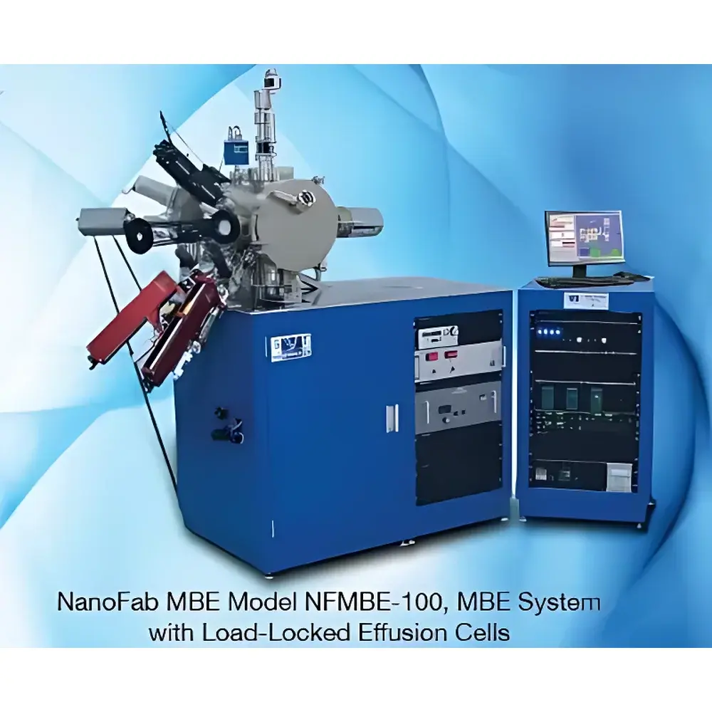
SMART NanoFab Compact Molecular Beam Epitaxy System
| Origin | USA |
|---|---|
| Manufacturer Type | Authorized Distributor |
| Origin Category | Imported |
| Model | SMART NanoFab |
| Pricing | Upon Request |
| Source Capacity | 4 or 8 effusion cells / e-beam sources |
| Integrated In-situ Monitors | RHEED, QCM, Linear Beam Flux Monitor |
| Growth Modes | Thermal Evaporation, E-beam Evaporation, RF Plasma, Pulsed Laser Deposition (PLD), Sputtering, Gas-Phase Precursor Delivery |
| Compatible Materials | III–V (e.g., GaAs, InP), II–VI (e.g., CdTe, ZnSe), II–Oxides (e.g., ZnO), III–Nitrides (e.g., GaN, AlN), and other compound semiconductors |
Overview
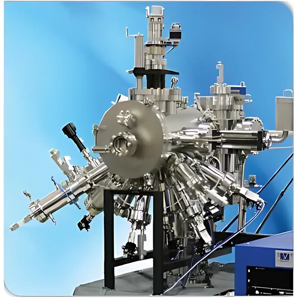
The SMART NanoFab Compact Molecular Beam Epitaxy (MBE) System is an ultra-high vacuum (UHV) thin-film growth platform engineered for precision epitaxial synthesis of compound semiconductor heterostructures. Unlike conventional MBE systems requiring dedicated cleanroom infrastructure and multi-square-meter footprints, the SMART NanoFab integrates full UHV MBE functionality—including effusion cell arrays, electron-beam evaporation, plasma-assisted sources, and pulsed laser ablation—within a compact, desktop-scale chamber (<0.5 m³ volume). Its core architecture adheres to fundamental MBE principles: molecular beam generation under UHV conditions (<5×10⁻¹⁰ Torr base pressure), line-of-sight deposition onto heated substrates, and real-time surface structural monitoring via Reflection High-Energy Electron Diffraction (RHEED). Designed for research laboratories with space constraints and multi-material exploration needs, it supports both stoichiometric control and kinetic-limited growth regimes essential for quantum well, superlattice, and 2D material fabrication.
Key Features
- Modular UHV chamber (stainless steel, all-metal seals, ISO-KF and CF flanges) with integrated bake-out system (up to 200 °C) enabling rapid pump-down and stable base pressure maintenance.
- Configurable source manifold accommodating either 4 or 8 independent thermal effusion cells, dual e-beam evaporators (with water-cooled crucibles), RF plasma source (13.56 MHz, up to 500 W), Nd:YAG pulsed laser ablation (266/532 nm, 10 Hz, <10 ns pulse width), DC/RF magnetron sputtering head, and gas injection nozzles for reactive precursors (e.g., NH₃, O₂, SiH₄).
- Dual-loadlock configuration: front-load sample transfer chamber (holds up to 6 × 2″ wafers or 12 × 10 mm² chips) with inert-gas purged glovebox interface, ensuring oxide-free substrate handling prior to UHV insertion.
- Integrated RHEED system (15–25 kV electron gun, phosphor screen + CCD camera) with AccuFlux™ real-time intensity analysis software for layer-by-layer growth mode verification and oscillation period quantification.
- In-situ metrology suite: quartz crystal microbalance (QCM) with ±0.001 Å/s resolution, linear beam flux monitor for absolute atomic flux calibration, and optional residual gas analyzer (RGA) for partial pressure tracking during reactive growth.
- Unified electronics cabinet housing programmable PID temperature controllers (substrate heater: 50–900 °C; cell ovens: RT–1300 °C), mass flow controllers (MFCs), high-voltage supplies, and synchronized data acquisition (16-bit ADC, 1 kHz sampling).
Sample Compatibility & Compliance
The SMART NanoFab accommodates standard semiconductor substrates including Si (100), GaAs (100), InP (100), sapphire (0001), and SiC (0001), with wafer sizes up to 2 inches and custom chip carriers for small-area device prototyping. Substrate heating utilizes resistive tantalum heaters with optical pyrometry feedback for ±1 °C thermal stability. All wetted materials comply with ASTM F2627 (UHV-compatible stainless steel grades) and ISO 14644-1 Class 4 cleanroom requirements when operated within appropriate enclosures. The system architecture supports GLP-compliant operation through audit-trail-enabled software logging (timestamped parameter sets, sensor readings, and user actions), and optional 21 CFR Part 11 compliance packages are available for regulated R&D environments.
Software & Data Management
Control is executed via NanoFabControl™ — a Windows-based, deterministic real-time application built on LabVIEW Real-Time Module. It provides synchronized sequencing of temperature ramps, shutter actuation, flux modulation, and in-situ signal capture. All RHEED oscillation data, QCM rate outputs, and beam flux profiles are time-stamped and stored in HDF5 format for interoperability with Python (NumPy/Pandas), MATLAB, and OriginLab. Export modules support ASTM E1394-compliant data exchange and CSV/TXT for legacy QC systems. Remote monitoring via secure TLS-encrypted web interface (HTTPS) enables off-site supervision without compromising firewall integrity.
Applications
- Growth of lattice-matched and strained III–V heterostructures (e.g., InGaAs/GaAs quantum wells for photodetectors and lasers).
- Epitaxial synthesis of wide-bandgap nitrides (AlGaN/GaN) on Si or sapphire for power electronics and UV optoelectronics.
- Atomic-layer-controlled oxide thin films (e.g., SrTiO₃, LaAlO₃) for complex oxide heterointerfaces and emergent phenomena studies.
- Hybrid growth integration: sequential MBE + PLD for metastable phase stabilization (e.g., BiFeO₃ on SrTiO₃).
- Rapid process development for novel chalcogenide (e.g., MoS₂, WSe₂) and topological insulator (e.g., Bi₂Se₃) monolayers using shuttered elemental co-evaporation.
- Calibration-grade thin-film reference standards for XRD, XPS, and TEM cross-section validation.
FAQ
What vacuum level does the SMART NanoFab achieve, and how is it maintained?
Base pressure ≤5×10⁻¹⁰ Torr is attained using a combination of turbomolecular pumps (≥800 L/s N₂ speed), ion getter pumps (1500 L/s), and non-evaporable getter (NEG) strips. Continuous pressure stability is ensured by active bake-out control and leak-tight all-metal sealing.
Can the system be upgraded to include additional in-situ characterization tools?
Yes — the chamber includes standardized CF-63 and CF-100 ports reserved for future integration of AES, XPS, or low-energy electron microscopy (LEEM) modules without structural modification.
Is remote operation supported for multi-user lab environments?
The system supports concurrent local and remote access via role-based authentication (admin/operator/viewer), with session logging and parameter change history traceable to individual users.
How is stoichiometry controlled during multi-source growth?
Flux calibration is performed using RHEED intensity oscillations combined with QCM rate cross-validation. NanoFabControl™ implements closed-loop shutter timing algorithms that dynamically adjust cell temperatures to maintain target group-V/group-III ratios within ±1.5% over 10-hour runs.
What maintenance intervals are recommended for UHV components?
Ion pumps require annual rejuvenation; turbomolecular pump oil replacement is scheduled every 12,000 operating hours; RHEED phosphor screens are rated for >5×10⁶ electron exposures before luminosity decay exceeds 20%. Full preventive maintenance is documented per ISO/IEC 17025 guidelines.


