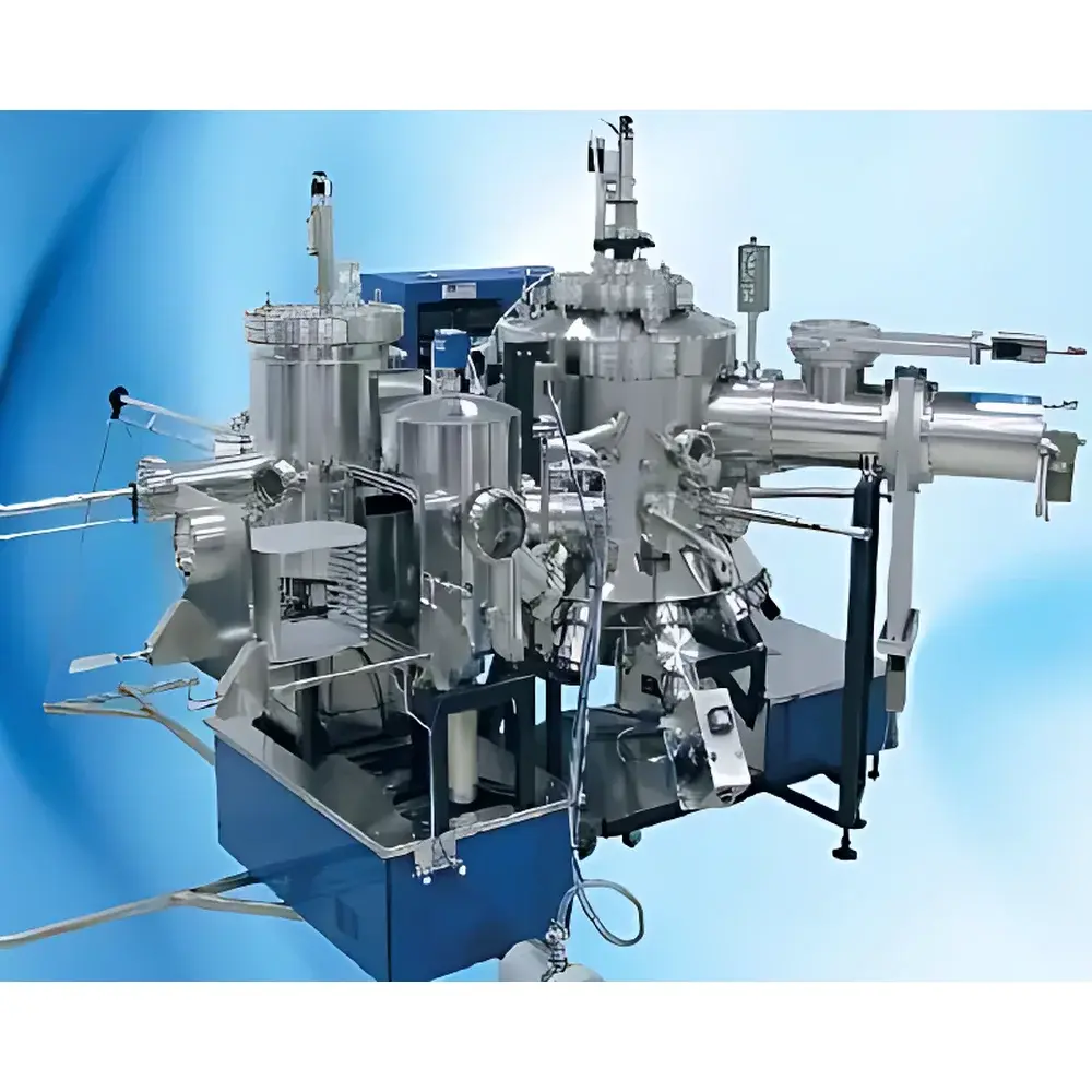
SVT 35V14 Production-Scale Molecular Beam Epitaxy System
| Origin | USA |
|---|---|
| Manufacturer Type | Authorized Distributor |
| Origin Category | Imported |
| Model | 35V14 |
| Pricing | Available Upon Request |
Overview
The SVT 35V14 Production-Scale Molecular Beam Epitaxy (MBE) System is an ultra-high-vacuum (UHV) thin-film growth platform engineered for reproducible, atomic-layer-precise epitaxial synthesis of compound semiconductor heterostructures. Based on Knudsen cell effusion sources and in situ reflection high-energy electron diffraction (RHEED), the system enables real-time monitoring and control of layer-by-layer growth kinetics under base pressures routinely below 2 × 10⁻¹⁰ Torr. Designed for transition from R&D to pilot-line and low-volume production environments, the 35V14 integrates industrial-grade vacuum architecture, thermal management redundancy, and modular source configuration to support sustained operation across extended deposition campaigns—critical for process qualification, material library development, and device prototyping in advanced optoelectronics, RF power electronics, and quantum materials research.
Key Features
- Large-area substrate capability: Accommodates wafers up to 14 inches (355 mm) in diameter with uniform temperature distribution across ±1.5 °C at growth temperatures up to 950 °C.
- High-throughput effusion source array: Configurable with up to 16 independently controlled Knudsen cells, including high-flux sources for Group III (Al, Ga, In), Group V (As, P, Sb), and reactive elements (O, N via plasma dissociation).
- Integrated RF-driven 6.0 kW Plasma Source: Enables stable, high-dissociation-rate atomic nitrogen and oxygen generation for growth of high-k dielectrics (e.g., Al₂O₃, HfO₂), III-nitrides (GaN, AlN), and complex oxides (e.g., STO, LNO).
- UHV chamber architecture: All-metal sealed, bakeable to 150 °C; equipped with dual-stage cryopumping (2000 L/s He-cooled cryopanels), ion getter pumps, and turbomolecular backing pumps ensuring rapid pump-down and long-term pressure stability.
- In situ diagnostics suite: Includes RHEED with auto-calibrated phosphor screen and CCD acquisition, quadrupole mass spectrometer (QMS) for partial pressure analysis, and pyrometry-based wafer temperature feedback control.
- Modular load-lock integration: Optional cassette-based load-lock system compliant with SEMI E10 standards supports automated wafer transfer without breaking main chamber vacuum.
Sample Compatibility & Compliance
The 35V14 supports heterogeneous substrate families including Si (100)/(111), GaAs (100), InP (100), sapphire (0001), SiC (4H- or 6H-SiC), and flexible metal foils (Ni, Mo) for transferable epitaxy. Substrate heating employs resistive backside heating with closed-loop PID control and emissivity-compensated pyrometry. The system complies with ISO 14644-1 Class 5 cleanroom interface requirements and meets mechanical safety standards per ANSI/UL 61010-1. Vacuum components conform to ASTM F2789 for UHV-compatible stainless steel (316L EP finish) and all electrical subsystems are CE-marked for EMC and low-voltage directive compliance.
Software & Data Management
Control and data acquisition are managed via SVT’s proprietary MBE-Studio™ software—a deterministic, real-time operating system (RTOS)-based platform supporting synchronized logging of >200 process parameters at 10 Hz resolution. Software features include recipe-driven growth sequencing, interlock logic for source shutter coordination, automated RHEED intensity tracking, and timestamped audit trails compliant with FDA 21 CFR Part 11 (electronic signatures, user access tiers, and immutable data archiving). Raw data exports to HDF5 and CSV formats; integration with LabVIEW and Python APIs enables custom analytics pipelines for growth rate modeling, stoichiometry prediction, and defect density correlation.
Applications
- Growth of lattice-matched and strain-balanced III-V heterostructures for high-electron-mobility transistors (HEMTs) and photonic integrated circuits (PICs).
- Atomic-layer-deposited high-k gate dielectrics and interfacial passivation layers for next-generation CMOS and beyond-CMOS logic devices.
- Epitaxial synthesis of wide-bandgap nitride semiconductors (AlGaN, InGaN) for UV LEDs, laser diodes, and high-power RF amplifiers.
- Complex oxide heteroepitaxy (e.g., LaAlO₃/SrTiO₃, YBCO/CeO₂) for emergent phenomena studies and superconducting electronics.
- Quantum well, quantum dot, and 2D material (e.g., TMDC monolayer) heterostructure fabrication requiring sub-monolayer thickness control and sharp interface definition.
FAQ
What vacuum level does the 35V14 achieve, and how is it maintained during extended runs?
Base pressure ≤2 × 10⁻¹⁰ Torr is achieved after 24-hour bakeout; continuous operation maintains ≤5 × 10⁻¹⁰ Torr via active cryopump regeneration cycles and ion pump current monitoring.
Can the system be upgraded to support in situ X-ray photoelectron spectroscopy (XPS)?
Yes—the chamber includes two 8-inch CF ports with UHV-compatible flanges and feedthroughs pre-wired for optional XPS or AES integration.
Is remote operation supported for multi-site facilities?
Fully supported via TLS-encrypted VNC tunneling with role-based access control; all critical alarms trigger SMS/email notifications through configurable SCADA gateway.
Does SVT provide process transfer support for existing MBE recipes?
Yes—SVT offers on-site recipe migration services including source flux calibration, RHEED pattern benchmarking, and cross-platform growth rate validation against legacy systems.
What maintenance intervals are recommended for the RF plasma source?
Plasma source electrodes require inspection every 500 operational hours; quartz window replacement is scheduled at 2000-hour intervals based on optical transmission decay measurements.


