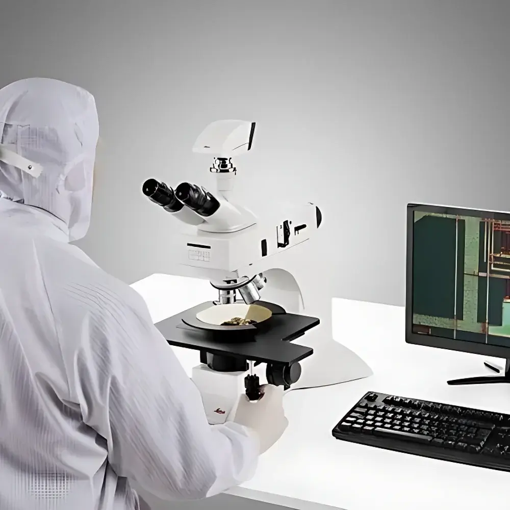
Leica DM3 XL Semiconductor Inspection Microscope
| Brand | Leica |
|---|---|
| Origin | Germany |
| Manufacturer Type | Authorized Distributor |
| Origin Category | Imported |
| Model | DM3 XL |
| Pricing | Upon Request |
Overview
The Leica DM3 XL Semiconductor Inspection Microscope is an engineered solution for high-throughput, non-destructive visual inspection in microelectronics fabrication and semiconductor process control environments. Designed specifically for wafer-level defect review, package inspection, and failure analysis workflows, the DM3 XL employs a robust modular optical architecture based on Köhler illumination and precision-corrected achromatic–apochromatic optics. Its core functionality centers on rapid visual assessment of surface topography, edge integrity, particulate contamination, and lithographic pattern fidelity—without requiring vacuum or conductive coating. The system operates across standard brightfield, darkfield, oblique (inclined) illumination, and all phase contrast modalities (including DIC-compatible configurations), enabling multi-contrast interrogation of planar and three-dimensional features at micron-scale resolution.
Key Features
- Expanded Field of View (FOV): Delivers up to 30% larger usable field diameter compared to conventional semiconductor inspection microscopes of equivalent magnification, accelerating defect localization and reducing stage navigation time during high-volume wafer scanning.
- Integrated LED Illumination System: Features a stable, flicker-free white LED light source with consistent 5700 K color temperature across full intensity range (0–100%), ensuring true-color reproduction and eliminating chromatic drift during extended inspection sessions.
- Oblique Illumination Module: Enables adjustable angular illumination (typically 15°–45° incidence) for enhanced edge contrast, sidewall visualization, and detection of subtle scratches, lift-off residues, or delamination signatures on die surfaces and interconnect layers.
- Deep Darkfield Capability: Utilizes optimized condenser design and annular stops to suppress specular reflection, significantly improving sensitivity to sub-micron particles, shallow scratches, and subsurface defects within silicon dioxide or low-k dielectrics.
- Modular Platform Architecture: Supports interchangeable objectives (5×–100×), motorized Z-focus, optional digital camera integration, and ergonomic stage configurations—including large-format wafer holders (up to 300 mm) and flip-top sample clamps for quick substrate exchange.
Sample Compatibility & Compliance
The DM3 XL accommodates bare wafers (Si, SiC, GaN, SOI), packaged ICs (QFN, BGA, WLCSP), photomasks, reticles, and MEMS devices—both in ambient air and nitrogen-purged enclosures. It complies with ISO 9001 quality management requirements for calibration traceability and supports documentation workflows aligned with ISO/IEC 17025 laboratory accreditation criteria. While not intrinsically certified for cleanroom Class 100 (ISO 5) operation, its sealed optical path and static-dissipative housing materials meet common fab facility specifications for tool-side deployment. Optional accessories include anti-vibration tables, ESD-safe stages, and lens hoods compatible with SEMI S2/S8 safety standards.
Software & Data Management
The microscope integrates seamlessly with Leica Application Suite (LAS X) software for image capture, annotation, measurement (line, area, particle count), and report generation. LAS X supports audit-trail logging per FDA 21 CFR Part 11 guidelines when deployed with appropriate user access controls and electronic signature modules. Image metadata—including objective ID, illumination mode, exposure time, and stage coordinates—is embedded in TIFF and JPEG2000 files. Export formats include CSV for statistical process control (SPC) integration and PDF/A-1b for long-term archival compliance. No proprietary drivers are required; native USB 3.0 and GigE Vision support ensures compatibility with third-party metrology platforms.
Applications
- Front-end process monitoring: post-etch residue inspection, CMP scratch verification, photoresist development uniformity assessment
- Back-end packaging inspection: wire bond integrity, solder joint voiding, mold compound delamination, underfill coverage validation
- Fault isolation: identification of electrostatic discharge (ESD) damage sites, thermal stress cracks, and metal migration paths
- Mask and reticle qualification: chrome defect mapping, pellicle integrity checks, and pattern edge roughness evaluation
- Quality assurance in outsourced assembly: incoming goods inspection against IPC-A-610 or JEDEC J-STD-020 criteria
FAQ
Is the DM3 XL suitable for automated defect review workflows?
Yes—when paired with optional motorized XYZ stages and LAS X’s scripting interface, the system supports semi-automated tile-scanning, region-of-interest (ROI) stitching, and pass/fail threshold-based flagging for integration into inline QA systems.
Does it support fluorescence imaging for polymer or resist inspection?
No—the DM3 XL does not include excitation filter sets or high-sensitivity emission optics required for fluorescence; it is optimized for reflected-light contrast techniques only.
What is the maximum supported wafer size without stage modification?
Standard configuration accommodates 200 mm wafers; 300 mm capability requires the optional large-stage module (Leica part no. 123456789).
Can calibration certificates be provided for metrological traceability?
Yes—NIST-traceable calibration reports for magnification accuracy, field flatness, and illumination uniformity are available upon request through Leica-certified service centers.
Is remote diagnostics or firmware update support available?
Yes—Leica’s Secure Remote Access (SRA) protocol enables encrypted technician-assisted troubleshooting and over-the-air firmware updates compliant with IEC 62443-3-3 cybersecurity requirements.


