Ellipsometry In-Line Monitoring System PMS by KJ GROUP
| Brand | KJ GROUP |
|---|---|
| Origin | Liaoning, China |
| Manufacturer Type | Authorized Distributor |
| Origin Category | Domestic (China) |
| Model | PMS |
| Pricing | Upon Request |
| Measurement Principle | Spectroscopic and Mueller Matrix Ellipsometry |
| Environmental Compatibility | Ambient Air, N₂ Atmosphere, Vacuum |
| Sample Environment Interface | Integrated vacuum flange or atmospheric port |
| Optical Range | 193–2500 nm (standard configuration: 380–1000 nm, extendable) |
| Measurement Modes | Variable-angle, Fixed-angle, Normal-incidence (vertical-angle) ellipsometry |
| Mapping Capability | Fully programmable X-Y stage with customizable travel range |
| Sample Size Support | Custom-engineered for large-format substrates (e.g., Gen 2–Gen 8.5 glass panels) |
| Single-Point Acquisition Time | 0.5–5 s (spectroscopic), <1 s (broadband fixed-angle) |
| Output Data | Thickness distribution maps, refractive index (n) & extinction coefficient (k) spatial profiles, layer stack modeling (Cauchy, Tauc-Lorentz, B-spline), real-time delta psi/delta delta contours |
| Software Compliance | Audit-trail enabled, user-level access control, data export in ASTM E2657-compliant CSV/HDF5 formats |
| Regulatory Alignment | Designed to support GLP/GMP-aligned process validation |
Overview
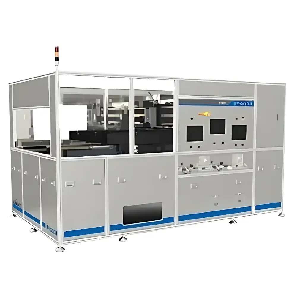
The KJ GROUP PMS Ellipsometry In-Line Monitoring System is an industrial-grade, spectroscopic and Mueller matrix ellipsometer engineered for real-time, non-contact, non-destructive characterization of thin-film structures on large-area substrates during semiconductor, flat-panel display (FPD), and advanced optoelectronic manufacturing. Operating on the fundamental principle of polarized light interaction—where incident p- and s-polarized components undergo phase shift (Δ) and amplitude ratio (Ψ) changes upon reflection from layered dielectric or absorbing films—the PMS system quantifies film thickness, optical constants (n, k), and interfacial roughness with sub-nanometer sensitivity. Unlike ex-situ benchtop ellipsometers, the PMS integrates directly into cleanroom production lines, supporting continuous monitoring under ambient air, nitrogen-purged, or high-vacuum environments (≤10⁻⁵ mbar). Its modular optical head architecture enables seamless integration with existing conveyor systems, robotic handling platforms, or inline vacuum chambers via standardized CF or ISO-K flanges.
Key Features
- Multi-modal ellipsometric detection: Simultaneous acquisition via spectroscopic ellipsometry (SE), Mueller matrix ellipsometry (MME), and reflectance-based film thickness metrology—enabling robust characterization of anisotropic, birefringent, or depolarizing stacks (e.g., PI alignment layers, patterned OLED emissive zones).
- Full spectral flexibility: Standard 380–1000 nm configuration; optional extension to deep UV (193 nm) and near-IR (2500 nm) supports critical applications including photoresist development monitoring, ITO carrier concentration profiling, and encapsulation layer absorption edge analysis.
- Configurable angular architecture: Three operational modes—variable-angle (15°–75°), fixed-angle (65° or 70°), and vertical-incidence (0°)—each optimized for throughput, sensitivity, or compatibility with constrained tool footprints.
- High-speed mapping engine: Programmable X-Y translation stage with ±5 µm repeatability; scan resolution down to 1 mm² per measurement point; full-wafer or Gen 8.5 (2200 × 2500 mm) substrate coverage achievable via custom travel path definition.
- Modular sensor interchangeability: Hot-swappable optical heads (SE, MME, reflectance) with factory-calibrated alignment—minimizing downtime during maintenance or process requalification.
Sample Compatibility & Compliance
The PMS accommodates rigid and semi-rigid planar substrates—including soda-lime glass, fused silica, quartz, and flexible polyimide-coated carriers—up to 2.5 m in diagonal dimension. It maintains measurement fidelity across multi-layer stacks comprising transparent conductive oxides (ITO, AZO), organic semiconductors (Alq₃, NPB), inorganic barriers (SiNₓ, Al₂O₃), and liquid crystal alignment polymers (PI). All hardware and firmware comply with IEC 61000-6-2/6-4 EMC standards. Software architecture supports traceable calibration logs, instrument qualification records (IQ/OQ/PQ), and electronic signatures per ASTM E2500-21 and ISO/IEC 17025:2017 requirements. Optional 21 CFR Part 11 add-on module provides role-based access control, electronic audit trails, and immutable raw-data archiving.
Software & Data Management
The proprietary KJ-EllipSoft™ platform delivers real-time data visualization, automated model fitting (using Levenberg-Marquardt and global optimization algorithms), and spatially resolved parameter mapping. Users define custom analysis templates—including Cauchy dispersion for wide-bandgap dielectrics, Tauc-Lorentz for amorphous silicon, or graded-interface B-spline models—and deploy them across batch runs. Raw spectra and fitted parameters are stored in HDF5 format with embedded metadata (timestamp, stage position, environmental pressure, lamp intensity). Batch reporting exports ASTM E2657-compliant PDF/CSV files containing statistical summaries (mean, σ, min/max), Cp/Cpk indices, and SPC control charts—directly ingestible into MES or SCADA systems.
Applications
- Flat-panel display manufacturing: Real-time monitoring of PI alignment layer uniformity (thickness ±0.2 nm, Δn < 0.005), photoresist bake/cure kinetics, and OLED pixel-defining bank structure integrity.
- Touch sensor fabrication: Quantification of ITO sheet resistance correlation with n/k dispersion, multilayer anti-reflection stack performance verification.
- Flexible electronics R&D: Thickness and optical anisotropy mapping of roll-to-roll coated barrier films under inert atmosphere.
- Micro-LED transfer bonding: Interfacial void detection via depolarization metrics derived from Mueller matrix decomposition.
- Encapsulation QA: In-line verification of ALD-grown Al₂O₃ moisture barrier thickness and stoichiometry on active-matrix backplanes.
FAQ
Can the PMS operate inside a vacuum chamber?
Yes—the optical head is available with CF-63 or CF-100 vacuum-compatible housing and feedthroughs for motorized stage control and fiber-optic signal transmission.
What is the minimum measurable film thickness?
Sub-monolayer sensitivity is achievable for high-contrast interfaces (e.g., SiO₂ on Si); typical resolution is 0.1 nm for single-layer SiNₓ on glass under optimized SE conditions.
Is third-party software integration supported?
Yes—KJ-EllipSoft™ provides RESTful API and OPC UA server interfaces for bidirectional communication with factory automation systems (SECS/GEM, MQTT, or Modbus TCP).
How is calibration traceability maintained?
Each system ships with NIST-traceable Si/SiO₂ reference wafers; field recalibration protocols follow ISO 15504-5 and include angle encoder verification, spectral radiance validation, and polarization state analyzer certification.
Does the system support automated defect-triggered re-measurement?
Yes—user-defined threshold logic (e.g., local k > 0.15 at 450 nm) can initiate targeted high-resolution rescan of flagged regions without interrupting line throughput.
Related Products


