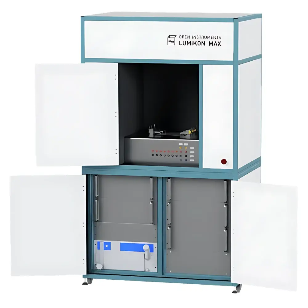
Open Instruments LUMiKON MAX Photoluminescence Imaging System for Solar Modules
| Brand | Open Instruments |
|---|---|
| Origin | Imported |
| Manufacturer Type | Authorized Distributor |
| Model | LUMiKON MAX |
| Trigger Mode | Steady-State |
| Camera Resolution | 61 MP |
| Pixel Size (with optional telecentric lens) | 3.6 µm/pixel |
| Uniformity | <5% |
| Sample Stage Compatibility | Si, Perovskite, Perovskite/Si Tandem (23 × 23 cm), Upgradable to Triple-Junction & III–V Devices |
| Illumination Range | 0.01–1.2 suns (AM1.5G equivalent) |
| Optional Features | Temperature-Controlled Stage, IBC-Compatible Stage, Lock-in Thermography (DLI-T), Point-Scan TRPL Spectroscopy, N₂ Enclosure with Real-Time Humidity/Temperature Monitoring |
| Software | Python-API Enabled, iVoc Imaging, Time-Normalized PL Analysis, iFF/iMPP/Pseudo-JV Extraction |
Overview
The Open Instruments LUMiKON MAX is a research-grade photoluminescence (PL) and electroluminescence (EL) imaging platform engineered for quantitative, spatially resolved characterization of photovoltaic devices—from single-junction silicon and perovskite cells to complex tandem and multi-junction architectures. Operating on the physical principle of radiative recombination imaging, the system captures near-infrared (NIR) PL emission under controlled optical excitation, enabling non-contact mapping of minority carrier lifetime, defect density distribution, local voltage loss (via calibrated iVoc imaging), and bandgap variation across full-size modules (up to 23 × 23 cm). Its design reflects deep domain expertise in emerging PV technologies, rooted in the foundational work of UNSW’s School of Photovoltaic and Renewable Energy Engineering—particularly in perovskite stability, interfacial recombination, and tandem cell optoelectronic losses.
Key Features
- Multi-modal imaging capability: Simultaneous or sequential acquisition of PL, EL, series resistance (Rs), Suns-Voc, pseudo-Jsc, time-resolved PL (TRPL), lock-in thermography (DLI-T), and point-spectrum-resolved lifetime mapping.
- High-fidelity optical architecture: 61 MP scientific CMOS sensor coupled with motorized telecentric optics; optional high-magnification lenses achieve 3.6 µm/pixel spatial resolution—enabling sub-cell grain-level analysis in perovskite thin films and interface-defect localization in heterojunctions.
- Automated metrology workflow: Precision kinematic stage with repeatability < 0.5 mm; auto-focus, auto-exposure, auto-filter wheel control, and programmable sample alignment—reducing operator dependency and improving inter-lab reproducibility.
- Calibrated iVoc imaging module: Enables quantitative, contactless determination of local open-circuit voltage (Voc) across incomplete or encapsulated devices—critical for process development and yield analysis without metallization or electrode patterning.
- Modular environmental control: Optional N₂-purged enclosure with integrated temperature/humidity sensors supports degradation studies under controlled atmospheres; compatible with thermal cycling (−40 °C to +85 °C) and illumination pre-biasing protocols per IEC 61215-2 MQT 19 and ISOS-D-3 standards.
Sample Compatibility & Compliance
The LUMiKON MAX accommodates standard and next-generation PV substrates including monocrystalline silicon (c-Si), polycrystalline silicon, CIGS, organic photovoltaics (OPV), and all perovskite-based architectures—especially perovskite/silicon tandems up to 23 × 23 cm. Its mechanical stage design supports both standard grid-patterned and interdigitated back-contact (IBC) configurations. The system meets core requirements for GLP-compliant lab environments: audit-trail-enabled software logging, user-access controls, electronic signature support (FDA 21 CFR Part 11 ready), and traceable calibration routines for intensity, spatial scale, and spectral response. All optical components are certified for NIR transmission (700–1100 nm), with quantum efficiency >75% at 1000 nm.
Software & Data Management
LUMiKON Control Suite provides a unified interface for instrument orchestration, experiment scripting, and real-time data visualization. It delivers native support for time-normalized PL decay fitting, pixel-wise iVoc extraction using calibrated reference diodes, and automated generation of iFF (internal fill factor), iMPP (internal maximum power point), and pseudo-JV curves. Raw image stacks are stored in HDF5 format with embedded metadata (exposure, bias, temperature, filter ID, timestamp). A documented Python API enables integration with custom analysis pipelines—including machine learning–based defect classification, statistical process control (SPC) dashboards, and cross-platform correlation with IV curve tracers or QE systems. Offline analysis licenses allow post-acquisition processing on dedicated workstations without hardware connection.
Applications
- Process optimization: Spatial correlation of PL quantum yield with deposition parameters (e.g., annealing temperature, anti-solvent dripping timing) in perovskite film fabrication.
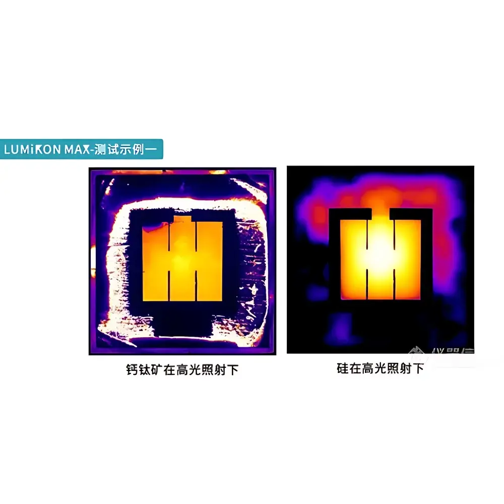
- Tandem cell diagnostics: Quantifying bottom-cell absorption losses, top-cell shunt pathways, and interlayer recombination via spectrally resolved PL and DLI-T co-registration.
- Encapsulant-induced degradation: Tracking localized PL quenching over accelerated damp-heat (DH) or UV exposure cycles inside inert atmosphere chambers.
- Module-level quality assurance: Identifying micro-cracks, solder bond failures, and edge delamination through differential PL/EL contrast mapping prior to lamination.
- Fundamental recombination physics: Extracting spatially resolved τeff maps from TRPL sequences and correlating them with cathodoluminescence or EBIC data.
FAQ
What excitation sources are supported?
The system integrates tunable LED arrays (365–940 nm) and optional laser diodes (e.g., 532 nm, 785 nm) for wavelength-specific excitation—enabling band-selective probing of perovskite sub-bandgap states or silicon bulk defects.
Can it measure full-size commercial modules (e.g., 1.7 m × 1.1 m)?
No—the current optical field-of-view is optimized for laboratory-scale samples up to 23 × 23 cm; larger-area mapping requires stitching routines (available as an add-on software module) with sub-pixel registration accuracy.
Is calibration traceable to NIST or PTB standards?
Yes—intensity calibration uses NIST-traceable silicon photodiode references; spatial calibration employs certified reticles; lifetime calibration is validated against standardized fluorescent reference standards (e.g., Rhodamine B in ethanol).
Does the system support automated pass/fail binning based on PL uniformity thresholds?
Yes—customizable pass/fail criteria can be defined per region-of-interest (ROI), with exportable CSV reports compliant with SPC frameworks (e.g., ASTM E2913).
What computing resources are required for real-time TRPL analysis?
A minimum of 64 GB RAM, dual Xeon CPUs, and NVIDIA RTX A6000 GPU are recommended for on-the-fly mono- and bi-exponential decay fitting across 61 MP frames at ≥10 fps acquisition rates.