ZEISS Gemini Series Field Emission Scanning Electron Microscope
| Brand | ZEISS |
|---|---|
| Origin | Germany |
| Instrument Type | Floor-standing / Conventional Large-format SEM |
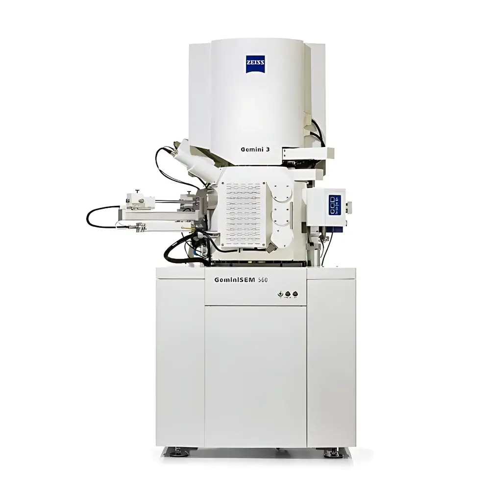
| Model | Gemini |
| Key Features | High-efficiency in-lens detection |
| Sample compatibility | Conductive & non-conductive, magnetic & non-magnetic, bulk & coated specimens |
| Compliance | Designed for ISO/IEC 17025-compliant labs |
Overview
The ZEISS Gemini Series is a high-performance field emission scanning electron microscope (FE-SEM) engineered for sub-nanometer resolution imaging and quantitative microstructural analysis across diverse scientific and industrial domains. Built upon ZEISS’s proprietary Gemini electron optical column — featuring a cold field emission gun (CFEG), aberration-optimized electrostatic-magnetic hybrid lenses, and a fully demagnetized objective lens system — the platform delivers exceptional signal-to-noise ratio, high collection efficiency, and stable beam performance at accelerating voltages ranging from 0.1 kV to 30 kV. Unlike conventional thermionic or Schottky-emission SEMs, the Gemini architecture enables true low-kV surface-sensitive imaging without compromising spatial resolution or signal fidelity, making it particularly suitable for beam-sensitive, uncoated, or magnetic specimens where charge accumulation or Lorentz deflection would otherwise degrade image quality.
Key Features
- Sub-nanometer resolution at 1 kV (≤0.8 nm), verified per ISO 16700:2016 test protocols using Au/Pt nanoparticles on carbon film
- InLens secondary electron (SE) detector integrated coaxially within the objective lens, maximizing collection efficiency for topographic contrast and edge enhancement
- Energy-selective backscattered (EsB) detector enabling compositional contrast separation with <5 eV energy window resolution
- Annular backscattered (aBSD) detector optimized for crystallographic contrast and channeling contrast in polycrystalline materials
- Zero-field objective lens design — eliminates magnetic interference, permitting direct imaging of ferromagnetic alloys, FeMn nanoparticles, and other magnetically hard materials without sample demagnetization or tilting artifacts
- Modular vacuum architecture supporting rapid sample exchange (<90 s pump-down from atmosphere to <1×10⁻⁶ mbar) and multi-chamber configurations for correlative workflows
Sample Compatibility & Compliance
The Gemini Series accommodates a broad spectrum of specimen types without mandatory conductive coating: insulating polymers, biological tissues (e.g., freeze-fractured mouse brain sections), battery cathode particles (NCM622), zeolite-embedded Ag nanoclusters, and FinFET semiconductor cross-sections. Its variable pressure mode (NanoVP) extends usability to partially hydrated or outgassing samples (e.g., uncoated photoresist on glass wafers). The system complies with IEC 61000-6-3 (EMC emissions) and IEC 61000-6-4 (industrial immunity), and its software architecture supports 21 CFR Part 11–compliant electronic signatures and audit trails when configured with ZEISS SmartSEM Enterprise Edition. Routine operation meets ISO/IEC 17025 requirements for accredited materials testing laboratories, including traceable calibration of magnification, working distance, and stage positioning.
Software & Data Management
Controlled via ZEISS SmartSEM software (v8.x), the Gemini platform provides deterministic acquisition scripting, multi-detector synchronization, and real-time drift correction using fiducial-based image registration. All acquired data — including raw TIFF stacks, metadata-rich .cor files (containing kV, WD, dwell time, detector gain, stage coordinates), and annotated measurement reports — are stored in vendor-neutral formats compliant with the EMDB (Electron Microscopy Data Bank) metadata schema. Optional ZEISS Atlas 5 enables automated large-area mosaic stitching (>100 mm²), particle analysis (size, shape, distribution), and integration with third-party tools such as Python-based PyXEM for diffraction pattern indexing or MATLAB for custom quantification pipelines.
Applications
- Materials Science: Grain boundary mapping in Ni-based superalloys, porosity quantification in additively manufactured Ti-6Al-4V, and in situ oxidation studies of Mg alloys under controlled gas environments
- Battery Research: Cross-sectional analysis of solid-electrolyte interphase (SEI) layers on Si anodes, degradation tracking of NCM811 cathodes after 500+ charge/discharge cycles, and lithium dendrite morphology assessment
- Semiconductor Metrology: Critical dimension (CD) verification of sub-5 nm logic nodes, gate oxide defect localization using voltage contrast imaging, and failure analysis of 3D NAND stack delamination
- Life Sciences: Serial block-face imaging of murine hippocampal tissue at 5 nm pixel size, immunogold labeling quantification on cryo-etched bacterial biofilms, and correlative light-EM (CLEM) alignment using fiducial markers
- Forensics & Cultural Heritage: Elemental fingerprinting of gunshot residue particles via EDS mapping, pigment layer stratigraphy in Renaissance oil paintings, and microfracture analysis of archaeological ceramics
FAQ
What vacuum level is required for optimal Gemini column performance?
The Gemini column operates at ultra-high vacuum (UHV) conditions: ≤2×10⁻⁸ mbar in the gun chamber and ≤5×10⁻⁷ mbar in the specimen chamber during high-resolution imaging. Turbo-molecular pumping with ion-getter backup ensures long-term stability.
Can the Gemini be integrated with EBSD or WDS systems?
Yes — the Gemini platform supports OEM-integrated Oxford Instruments AZtec EBSD and Horiba XGT-7200 WDS systems via standardized flange interfaces (CF100) and synchronized acquisition triggers.
Is training provided for regulatory-compliant operation?
ZEISS offers GLP-aligned operator certification programs covering instrument qualification (IQ/OQ/PQ), preventive maintenance logs, and 21 CFR Part 11 validation documentation packages upon request.
How does the NanoVP mode differ from conventional low-vacuum SEM?
NanoVP employs differential pumping with two-stage apertures and a dedicated gaseous secondary electron detector, enabling imaging at 10–100 Pa water vapor pressure while maintaining <1.5 nm resolution — significantly higher than typical low-vacuum SEMs operating above 100 Pa.
What is the maximum specimen size supported in standard configuration?
Standard Gemini stages accommodate specimens up to Ø100 mm × 50 mm height; extended-height chambers and motorized tilt-rotate stages support Ø150 mm wafers and irregularly shaped artifacts up to 200 mm in length.


