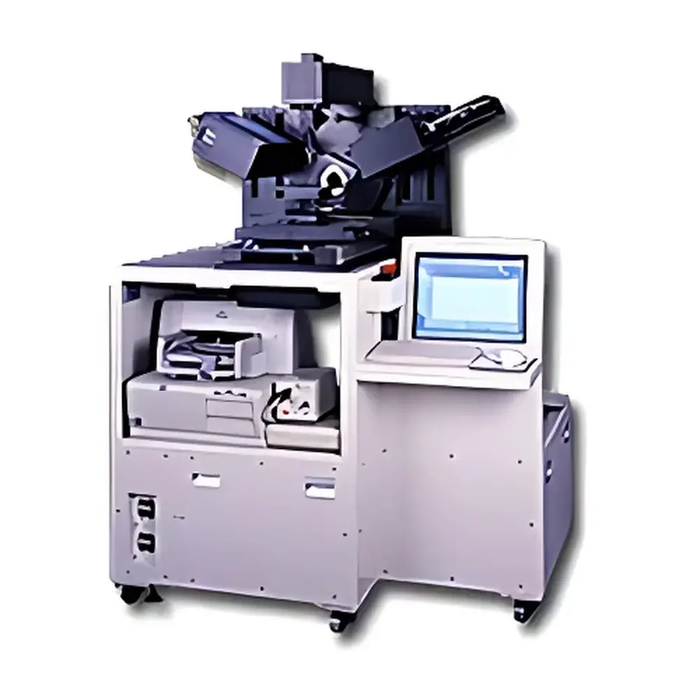
HalfMoon Auto Ellipsometer for Nanoscale Thin-Film Metrology
| Brand | HalfMoon |
|---|---|
| Origin | Japan |
| Supplier Type | Authorized Distributor |
| Import Status | Imported |
| Wavelength Range | 250–800 nm (optional 350–1000 nm) |
| Thickness Measurement Range | 0.1 nm to >10 µm |
| Detector | Thermoelectrically Cooled Photodiode Array, 512 channels |
| Angle of Incidence/Reflection | 45°–90° (motorized, fully adjustable) |
| Power Supply | AC 1500 VA |
| Dimensions (H×D×W) | 1300 × 900 × 1750 mm |
| Weight | ~350 kg |
| Measurement Principle | Spectroscopic Ellipsometry (SE) |
Overview
The HalfMoon Auto Ellipsometer is a high-precision, motorized spectroscopic ellipsometer engineered for non-destructive, sub-nanometer thickness and optical constant (n, k) characterization of thin films in semiconductor process development and manufacturing. Based on the fundamental principles of polarization-state modulation and differential reflection analysis, the system measures the change in ellipticity (Ψ) and phase shift (Δ) of polarized light upon interaction with a sample surface across a broad spectral range. Unlike intensity-based reflectometry, ellipsometry provides intrinsic sensitivity to both film thickness and complex refractive index—enabling robust quantification of ultrathin gate oxides (<1 nm), high-k dielectrics, amorphous and polycrystalline layers, and anisotropic stacks without physical contact or calibration standards. Its design prioritizes metrological traceability, thermal stability, and long-term repeatability—critical for process control in advanced node fabrication (e.g., FinFET, GAA, and memory technologies).
Key Features
- Full-spectrum spectroscopic ellipsometry from 250 nm to 800 nm (extendable to 350–1000 nm), supporting deep-UV lithography metrology (e.g., KrF at 248 nm, i-line at 365 nm)
- Motorized, programmable angle-of-incidence adjustment (45°–90°) to optimize signal-to-noise ratio and decouple thickness/optical constant correlations in multilayer systems
- Thermoelectrically cooled 512-channel photodiode array detector ensuring low dark-current noise and high spectral resolution for reliable Ψ/Δ extraction
- Automated stage and alignment routines enabling unattended operation in cleanroom environments (Class 100 or better)
- Non-linear least-squares regression engine for simultaneous fitting of multi-layer optical models—including dispersion-corrected Cauchy, Tauc-Lorentz, or B-spline parameterizations
- Integrated environmental monitoring (temperature, humidity) to compensate for drift during extended measurement sessions
Sample Compatibility & Compliance
The system accommodates standard semiconductor wafers up to 300 mm diameter, including patterned and blanket substrates. It supports measurement on Si, SiC, GaN, InP, sapphire, and glass substrates with native oxides, ALD/CVD/PVD-deposited films (e.g., SiO₂, SiNₓ, Al₂O₃, HfO₂, TiN, ITO, DLC), photoresists, and organic alignment layers. All hardware and software modules comply with ISO/IEC 17025 requirements for testing laboratories. Data acquisition and reporting conform to ASTM E1933-22 (Standard Practice for Spectroscopic Ellipsometry Measurements) and support audit-ready documentation per FDA 21 CFR Part 11 when deployed in regulated GMP/GLP environments.
Software & Data Management
The proprietary control and analysis suite includes real-time spectrum visualization, library-assisted model building, batch recipe management, and automated report generation (PDF/CSV). Raw Ψ/Δ spectra are stored in HDF5 format with embedded metadata (timestamp, instrument configuration, environmental logs). The software supports secure user role management, electronic signatures, and full audit trail functionality—including modification history of optical models and fit parameters. Integration with factory MES via SECS/GEM protocol enables direct feedback to process tools for closed-loop control.
Applications
- Semiconductor front-end: Gate oxide thickness uniformity mapping, high-k/metal gate stack composition profiling, interfacial layer detection in SiO₂/SiON/SiNₓ systems
- Compound semiconductor epitaxy: AlGaAs, InGaN, and SiC heterostructure layer thickness and bandgap grading
- Flat-panel display: ITO sheet resistance correlation, MgO protective layer density, polyimide alignment film birefringence
- Advanced packaging: Low-k dielectric integrity assessment (e.g., porous SiCOH), Cu barrier/adhesion layer thickness
- Lithography R&D: Photoresist optical constant dispersion modeling (n(λ), k(λ)) for OPC calibration and dose optimization
- Emerging materials: Superconducting YBCO films, magnetic tunnel junction (MTJ) spacer layers, and diamond-like carbon (DLC) hardness proxy via density-derived n
FAQ
Does this ellipsometer support measurement on patterned wafers?
Yes—via micro-spot optics (optional) and spatial averaging algorithms compatible with standard macro-ellipsometry configurations.
Can it measure ultra-thin films below 0.5 nm?
Yes—through high-SNR acquisition at optimal angles and constrained fitting using physically plausible dispersion models.
Is NIST-traceable calibration available?
Yes—certified Si/SiO₂ reference wafers (with certified thickness uncertainty <0.05 nm) are supplied with optional calibration service.
What level of automation is integrated?
Full automation includes auto-focus, auto-alignment, wafer centering, recipe-driven multi-site mapping, and error-recovery protocols.
How is data security ensured for regulated environments?
Role-based access control, encrypted local storage, electronic signature workflows, and 21 CFR Part 11-compliant audit trails are enabled by default.


