HalfMoon 01 Embedded Thin-Film Thickness Monitor
| Brand | HalfMoon |
|---|---|
| Origin | Japan |
| Model | 01 |
| Type | In-situ, Fiber-optic-based Spectroscopic Reflectometry System |
| Deployment | Inline/At-line Integration for Semiconductor Processing Equipment |
| Environmental Rating | Vacuum-Compatible (up to 1×10⁻⁶ Pa), Cleanroom Class 100 Certified |
| Measurement Principle | Broadband Spectral Reflectometry (400–1100 nm) with Real-time Interference Analysis |
Overview
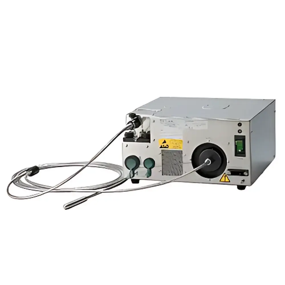
The HalfMoon 01 Embedded Thin-Film Thickness Monitor is an industrial-grade, fiber-coupled spectroscopic reflectometer engineered for real-time, non-contact thickness metrology of single- and multi-layer dielectric and semiconductor films during active fabrication processes. Designed explicitly for integration into semiconductor manufacturing tools—including CMP slurry delivery systems, PVD sputtering chambers, and plasma-enhanced CVD reactors—the system operates on the physical principle of spectral interference: broadband light (400–1100 nm) is delivered via armored, low-loss optical fiber to the sample surface; reflected intensity spectra are captured and analyzed in real time using a high-resolution CCD spectrometer and proprietary thin-film inversion algorithms. This enables sub-nanometer resolution in thickness determination for layers ranging from 5 nm to 5 µm—without interrupting process flow or requiring vacuum break. Its compact, modular architecture supports both normal-incidence and oblique-angle configurations, making it suitable for wafer-level mapping, glass substrate monitoring in display manufacturing, and inline control of anti-reflective, passivation, and gate dielectric stacks.
Key Features
- Fiber-optic integration architecture: Enables seamless mounting directly onto tool flanges, robotic end-effectors, or process chamber viewports without compromising vacuum integrity or thermal stability.
- Real-time, multi-point synchronous acquisition: Up to 8 independent measurement channels configurable via time-division multiplexing, each delivering full-spectrum data at ≥10 Hz frame rate under continuous operation.
- Vacuum-rated optical probe head: Constructed from 316L stainless steel and alumina ceramics; qualified for sustained operation at pressures down to 1×10⁻⁶ Pa and temperatures from −20 °C to +85 °C.
- Calibration traceability: Factory-calibrated against NIST-traceable SiO₂/Si reference wafers; supports user-defined calibration routines compliant with ISO/IEC 17025 requirements.
- Tool-to-tool interoperability: Equipped with SECS/GEM (SEMI E30/E37) and OPC UA (IEC 62541) interfaces for native integration into 300 mm fab automation frameworks (e.g., MES, APC).
Sample Compatibility & Compliance
The HalfMoon 01 supports in-situ measurement across silicon wafers (150 mm to 300 mm), fused silica and alkali-free glass substrates (Gen 2 to Gen 10), and compound semiconductor wafers (GaN-on-Si, SiC). It accommodates transparent, semi-transparent, and absorbing film systems—including SiO₂, SiNₓ, Al₂O₃, ITO, TiO₂, and amorphous Si—with no requirement for backside access or electrical contact. All hardware and firmware comply with SEMI S2/S8 safety standards, CE Machinery Directive 2006/42/EC, and RoHS 2011/65/EU. Software execution adheres to FDA 21 CFR Part 11 requirements for electronic records and signatures, including audit trail logging, role-based access control, and data immutability enforcement.
Software & Data Management
The embedded controller runs HalfMoon ThicknessSuite™ v4.2—a deterministic real-time OS (VxWorks 7) hosting calibrated spectral analysis engines, layer stack modeling tools (transfer-matrix method), and statistical process control (SPC) modules. Raw spectra and derived thickness values are streamed in HDF5 format with embedded metadata (timestamp, tool ID, recipe name, chamber pressure, temperature). Data synchronization supports local NVMe storage (2 TB RAID-1) and secure TLS 1.3 transmission to centralized data lakes. The software includes built-in support for ASTM F393-22 (Standard Practice for In-situ Optical Monitoring of Thin Films During Deposition) and provides automated report generation aligned with ISO 9001 quality documentation workflows.
Applications
- Endpoint detection and uniformity monitoring during plasma etch and reactive ion etching (RIE) of hard masks and interlayer dielectrics.
- Real-time feedback control of deposition rates in magnetron sputtering and atomic layer deposition (ALD) tools.
- Wafer-level thickness mapping for chemical mechanical polishing (CMP) endpoint verification and dishing/erosion quantification.
- Process qualification and drift tracking in high-volume display manufacturing (OLED, microLED) on large-area glass substrates.
- Qualification of barrier layer integrity in advanced packaging (e.g., TSV redistribution layers, fan-out wafer-level packaging).
FAQ
Is the HalfMoon 01 compatible with existing vacuum feedthroughs on standard semiconductor process tools?
Yes—its optical probe uses a standardized CF-35 or KF-40 flange interface with integrated ceramic-insulated fiber feedthroughs rated for UHV compatibility.
Can the system distinguish between overlapping layers with similar refractive indices?
Yes—by leveraging multi-angle reflectance modeling and spectral fitting residuals, it resolves layer thicknesses and optical constants (n, k) simultaneously for up to four-layer stacks.
Does the software support integration with factory-wide APC systems?
Yes—via native SECS/GEM messaging and OPC UA PubSub, enabling closed-loop control of deposition power, gas flow, and bias voltage based on real-time thickness deviation signals.
What is the minimum measurable thickness for ultra-thin ALD-grown HfO₂ films?
Under optimal signal-to-noise conditions (≥1000:1 SNR), the system achieves ±0.15 nm repeatability for films ≥2 nm thick, validated per SEMI D39-0218 test methodology.
How frequently does the system require recalibration in a production environment?
Factory calibration remains stable for ≥12 months under controlled cleanroom conditions; quarterly verification using certified reference wafers is recommended per ISO/IEC 17025 Clause 7.7.


