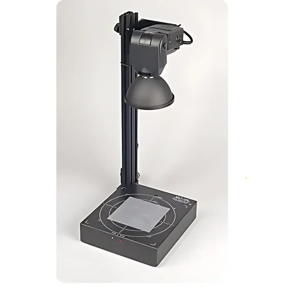
Rayscience WCT-120 Quasi-Steady-State Photoconductance (QSSPC) Minority Carrier Lifetime Tester
| Brand | Rayscience |
|---|---|
| Origin | USA |
| Manufacturer Type | Authorized Distributor |
| Origin Category | Imported |
| Model | WCT-120 |
| Measurement Principle | QSSPC (Quasi-Steady-State Photoconductance) |
| Lifetime Range | 100 ns – 10 ms |
| Test Modes | QSSPC, Transient, Lifetime Normalization Analysis |
| Resistivity Range | 3–600 Ω/sq. (undoped) |
| Carrier Injection Range | 1×10¹³ – 1×10¹⁶ cm⁻³ |
| Sensor Diameter | 40 mm |
| Sample Diameter | 40–210 mm (customizable down to smaller sizes) |
| Silicon Thickness | 10–2000 µm |
| Ambient Temperature | 20–25 °C |
| Power Consumption | Tester: 40 W |
| Controller PC | 200 W |
| Light Source | 60 W |
| Input Voltage | 100–240 VAC, 50/60 Hz |
Overview
The Rayscience WCT-120 is a high-precision, calibrated minority carrier lifetime tester engineered for quantitative recombination characterization of silicon wafers, ingots, and bricks in semiconductor and photovoltaic manufacturing environments. It implements the Quasi-Steady-State Photoconductance (QSSPC) method—a rigorously validated, non-contact, contactless technique first developed by Sinton Instruments in 1994 and widely adopted as an industry reference standard for lifetime metrology. Unlike transient photoconductance or microwave-detected photoconductance decay (µW-PCD), QSSPC provides direct, calibration-traceable measurement of effective minority carrier lifetime (τeff) across a broad injection range (1013–1016 cm−3), enabling physically meaningful interpretation of bulk and surface recombination kinetics. The system simultaneously derives the implied open-circuit voltage (iVOC) versus illumination intensity curve—functionally equivalent to a process-stage I-V characteristic—without requiring electrical contacts or device fabrication. This capability makes the WCT-120 indispensable for inline process development, material qualification, and root-cause analysis of efficiency-limiting recombination mechanisms.
Key Features
- QSSPC-based lifetime measurement with traceable calibration against NIST-traceable reference samples
- Integrated transient photoconductance mode for cross-validation and fast screening
- Automated, script-driven operation with full data logging, timestamping, and audit trail generation compliant with GLP/GMP requirements
- Support for unpassivated “as-cut” wafers—no mandatory surface treatment required prior to measurement
- Position-selective probing: user-defined measurement locations on wafers up to 210 mm diameter (standard 40 mm sensor aperture)
- Patent-protected optional chemical surface passivation module for controlled SiO2/HF-based钝化 (available upon request)
- Extended resistivity compatibility: functional down to 0.1 Ω·cm for low-resistivity Czochralski and cast-multicrystalline silicon
- Modular architecture supporting future upgrades including lifetime mapping (via motorized XY stage integration)
Sample Compatibility & Compliance
The WCT-120 accommodates raw and processed silicon substrates across the full PV and semiconductor value chain: monocrystalline and multicrystalline ingots (measured via edge or top-surface contact), sawn wafers (40–210 mm), kerf-loss-reduced thin wafers (10–2000 µm), diffusion-processed emitters, dielectric-coated surfaces (SiNx, Al2O3), and finished solar cells. All measurements comply with ASTM F1535–22 (“Standard Test Method for Minority-Carrier Lifetime of Silicon Wafers by Quasi-Steady-State Photoconductance”) and align with ISO 17025–2017 metrological requirements when operated under documented calibration and environmental control (20–25 °C ambient, <5% RH variation). System firmware supports 21 CFR Part 11-compliant electronic signatures and secure user access levels (admin/operator/auditor).
Software & Data Management
Control and analysis are executed via Rayscience’s proprietary LifetimeStudio™ software suite, built on a deterministic real-time acquisition engine. Each measurement generates a complete dataset including τeff(Δn), iVOC(Δn), surface recombination velocity (SRV) estimates (when paired with known surface passivation quality), and injection-level-normalized lifetime curves. Data export conforms to ASTM E2817–21 (Standard Practice for Data Exchange in Photovoltaic Metrology) and supports CSV, HDF5, and XML formats. Audit logs record operator ID, timestamp, instrument configuration, calibration certificate ID, and environmental sensor readings (temperature/humidity). Batch reporting tools enable statistical process control (SPC) charting per lot, furnace run, or tool ID—fully compatible with MES integration via OPC UA or REST API.
Applications
- Baseline material qualification of virgin ingots and wafers prior to processing
- In-line monitoring of diffusion uniformity and emitter saturation current density (J0e) estimation
- Quantitative assessment of surface passivation quality (e.g., Al2O3 ALD layers, SiNx PECVD stacks)
- Detection of metallic contamination (Fe, Cr, Cu) through lifetime degradation kinetics under controlled illumination
- Process-induced shunt detection via anomalous iVOC curvature at high injection
- Root-cause analysis of low-efficiency batches in PERC, TOPCon, and HJT cell lines
- Research-grade lifetime mapping (with optional XY stage) for grain boundary and defect cluster localization
FAQ
What is the recombination lifetime?
The minority carrier recombination lifetime (τ) quantifies the average time a photo-generated electron-hole pair persists before annihilation via radiative, Auger, or defect-mediated pathways. It directly governs the diffusion length (L = √(Dτ)) and thus the charge collection efficiency in photovoltaic devices.
How does solar cell efficiency depend on lifetime?
For silicon cells, efficiency scales approximately linearly with τ above ~100 µs in high-quality material; below this threshold, efficiency drops sharply due to increased recombination losses in the base and emitter regions.
What determines lifetime in silicon?
Bulk lifetime is governed primarily by transition-metal impurities (Fe, Cr, Cu), oxygen precipitates, and dislocation clusters. Surface lifetime depends on interface defect density (Dit) and chemical passivation quality.
How is lifetime measured by the WCT-120?
Using QSSPC: a stabilized LED light source generates steady-state excess carriers; the resulting photoconductance is measured via lock-in detection while modulating illumination intensity. τ is extracted from the slope of Δn vs. Δσ using the generalized Shockley–Read–Hall model.
Can the system measure surface recombination velocity (SRV)?
Yes—when combined with a known surface passivation structure (e.g., thermally grown SiO2), SRV is derived from the injection-dependent τ curve using the LeGrand–Sah formalism.
Does the instrument require sample passivation for valid measurement?
No. The WCT-120 delivers physically meaningful τ values on bare, uncoated wafers (“out-of-the-box”), though surface passivation improves sensitivity to bulk defects.
How is calibration performed?
Calibration employs certified reference wafers with lifetimes traceable to NIST Standard Reference Material (SRM) 2593, verified annually per ISO/IEC 17025 procedures. In-field verification uses built-in reference diodes and thermal drift compensation algorithms.
What is the smallest measurable sample size?
The standard 40-mm-diameter sensor requires ≥40 mm samples; however, custom apertures support measurements on fragments as small as 15 × 15 mm with reduced spatial resolution.


