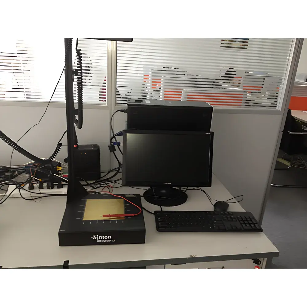
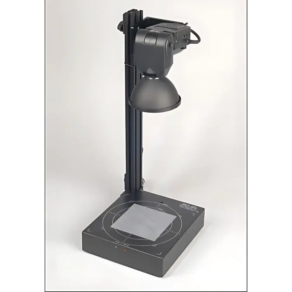
Sinton Instruments WCT-120 Quasi-Steady-State Photoconductance Minority Carrier Lifetime Tester
| Brand | Sinton Instruments |
|---|---|
| Origin | USA |
| Model | WCT-120 |
| Minority Carrier Lifetime Range | 0.1 µs – 15 ms |
| Penetration Depth | 3 mm |
| Sample Diameter | up to 210 mm |
| Resistivity Measurement Range | 0.15 – 300 Ω·cm |
| Test Material | Silicon Wafers |
Overview
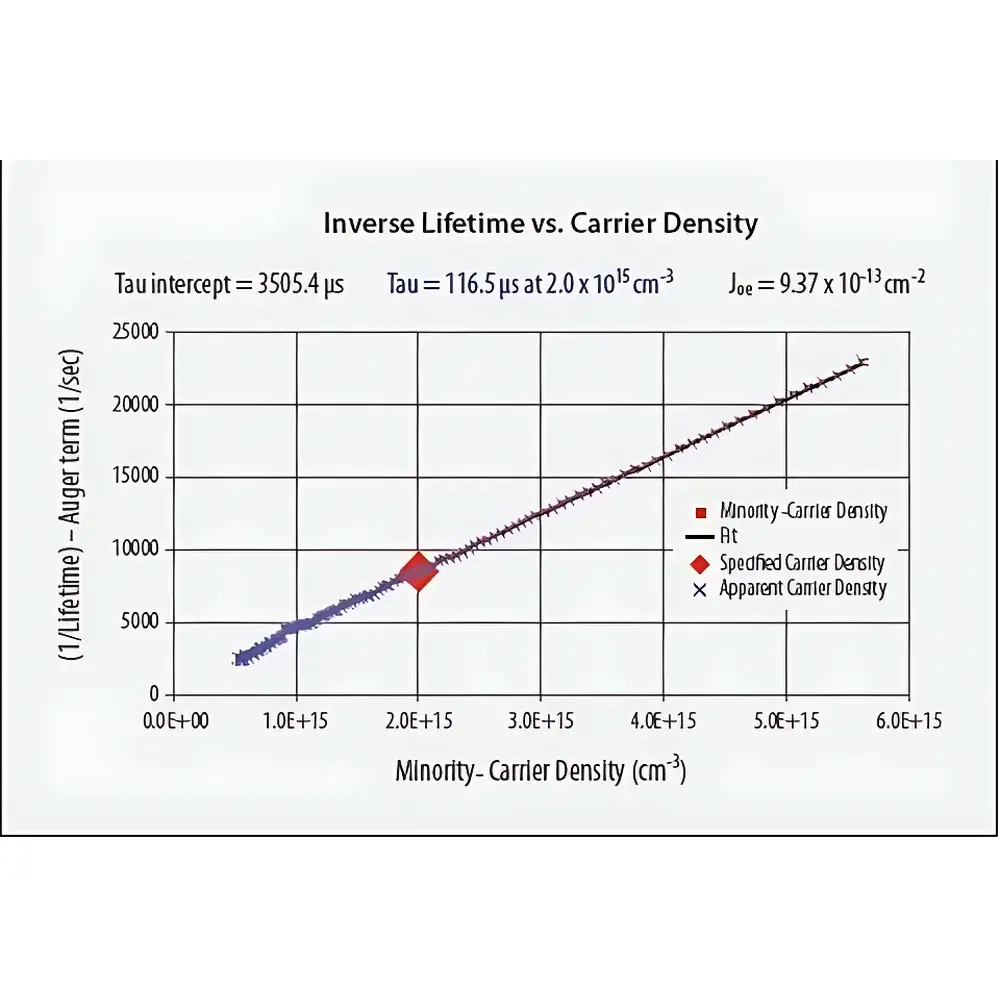
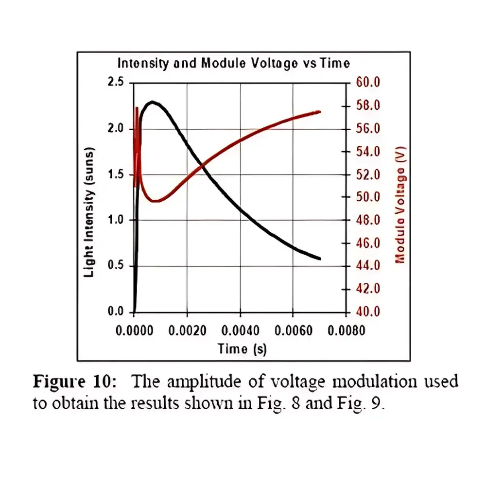
The Sinton Instruments WCT-120 is a high-precision, benchtop quasi-steady-state photoconductance (QSSPC) instrument engineered for quantitative, non-contact minority carrier lifetime (τeff) characterization of silicon wafers and bulk materials used in photovoltaic (PV) manufacturing and semiconductor R&D. Operating on the physical principle of photoconductance decay under controlled, stabilized illumination, the WCT-120 measures the effective recombination lifetime of minority carriers—primarily electrons in p-type silicon or holes in n-type silicon—by monitoring the transient photocurrent response following precise light injection. Unlike transient methods requiring ultrafast lasers or complex synchronization, QSSPC delivers high reproducibility at moderate cost and operational simplicity, making it the industry-standard technique for inline process control and material qualification across ingot, wafer, and cell fabrication lines. The system is calibrated traceably to NIST-reference standards and complies with ASTM F1534–22 (“Standard Test Method for Measuring Minority-Carrier Lifetime of Silicon Wafers by Quasi-Steady-State Photoconductance”) and ISO 12099:2017 (“Photovoltaic devices — Requirements for measuring minority-carrier lifetime in crystalline silicon”).
Key Features
- QSSPC-based measurement architecture optimized for industrial robustness and laboratory-grade accuracy
- Extended lifetime range: 0.1 µs to 15 ms, covering both low-quality as-grown ingots and high-efficiency passivated wafers
- Integrated resistivity mapping capability (0.15–300 Ω·cm), enabling concurrent doping uniformity assessment without sample transfer
- 3 mm optical penetration depth ensures bulk-sensitive evaluation for standard Czochralski (CZ) and float-zone (FZ) silicon wafers (10–2000 µm thick)
- Full-diameter scanning support for wafers up to 210 mm (8.25″), with optional stage positioning for localized spot measurements (≥1 mm resolution)
- Patented surface chemical passivation protocol included—enabling reliable τeff extraction on as-cut, uncoated, or metallized wafers without prior HF dip or ALD treatment
- Automated measurement sequence with embedded temperature stabilization (20–25 °C ambient operation recommended) and real-time drift compensation
Sample Compatibility & Compliance
The WCT-120 accommodates monocrystalline, multicrystalline, and cast-mono silicon substrates—including bare wafers, textured surfaces, SiNx/AlOx-passivated samples, and finished solar cells with front-side metallization. It supports routine QC testing across all PV production stages: ingot slicing verification, wafer incoming inspection, post-diffusion lifetime screening, passivation layer optimization, and final cell binning. All hardware and firmware meet CE marking requirements and are designed for compliance with GLP/GMP documentation workflows. Data integrity is maintained per FDA 21 CFR Part 11 when operated with validated software configurations, including electronic signatures, audit trails, and secure user access controls.
Software & Data Management
The instrument is controlled via Sinton’s proprietary LifetimeStudio™ software (Windows 10/11 compatible), which provides real-time waveform visualization, multi-parameter curve fitting (including SRH, Auger, and surface recombination modeling), batch reporting, and CSV/Excel export. Measurement data includes τeff, implied Voc, sheet resistance, and injection-level-dependent lifetime curves. Software supports automated report generation aligned with internal quality manuals and external customer requirements (e.g., IEC 61215, UL 1703). Raw data files are stored in open HDF5 format, ensuring long-term archival compatibility and third-party analysis interoperability.
Applications
- Process development and optimization of diffusion, passivation, and metallization steps
- Material grading of silicon feedstock and ingots prior to wafering
- In-line monitoring of saw damage recovery and gettering efficacy
- Qualification of PERC, TOPCon, and HJT cell architectures during R&D and pilot line validation
- Root-cause analysis of efficiency losses linked to bulk defects, metal contamination, or interfacial recombination
- Support for ISO/IEC 17025-accredited calibration laboratories performing third-party wafer certification
FAQ
What measurement principle does the WCT-120 use?
It employs quasi-steady-state photoconductance (QSSPC), where a stabilized LED light source generates a known excess carrier density, and the resulting photoconductance is measured via contactless eddy-current or microwave detection.
Can it measure wafers with anti-reflective coatings or metal contacts?
Yes—the system’s dual-wavelength excitation and adaptive signal processing enable accurate lifetime extraction on SiNx, AlOx, TiO2, and screen-printed Ag/Al layers without removal or masking.
Is resistivity measurement integrated into the same test cycle?
Yes; four-point probe resistivity (0.15–300 Ω·cm) is acquired simultaneously with lifetime, eliminating sequential instrumentation and alignment errors.
Does the system require vacuum or inert atmosphere operation?
No—it operates reliably in ambient air at controlled room temperature (20–25 °C); no gas purging or environmental chamber is needed.
What level of operator training is required?
Basic operation requires <2 hours of instruction; advanced analysis (e.g., recombination parameter extraction) is supported by built-in tutorials and Sinton’s application engineering team via remote assistance.


