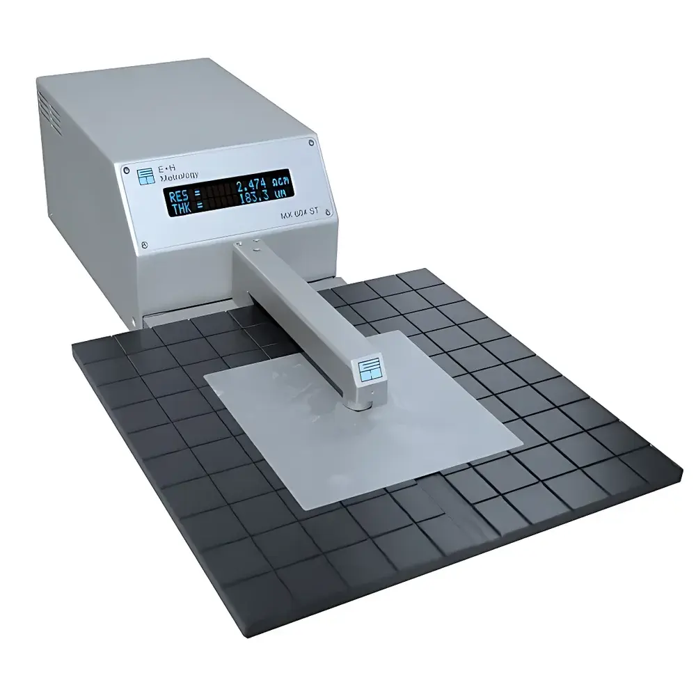
E+H Metrology MX604-ST Single-Point Wafer Thickness & Resistivity Tester
| Brand | E+H Metrology |
|---|---|
| Origin | Germany |
| Model | MX 604-ST |
| Wafer Diameter | 50–200 mm |
| Thickness Range | 60–300 µm or 250–750 µm |
| Thickness Accuracy | ±1 µm |
| Sensor Active Diameter | 8 mm |
| Sensor Housing Diameter | 20 mm |
| Edge Exclusion Distance | 10 mm |
| Measurement Time per Point | 0.3 s |
| Sheet Resistance Range | 10–2000 Ω/sq |
| Resistivity Range | 0.25–50 Ω·cm (at 250 µm) / 0.75–150 Ω·cm (at 750 µm) |
| Software | EHMaster |
Overview
The E+H Metrology MX604-ST is a single-point, non-contact metrology instrument engineered for simultaneous measurement of silicon and wide-bandgap semiconductor wafer thickness and bulk resistivity. It operates on the principle of eddy-current induction for resistivity determination and high-resolution capacitive sensing for thickness profiling—both methods compliant with established semiconductor process control methodologies. Designed for integration into front-end fab environments and final test laboratories, the MX604-ST delivers traceable, repeatable measurements without requiring physical contact, vacuum chucking, or backside metallization. Its architecture supports rapid point-based verification across full wafers (50–200 mm diameter), making it suitable for inline process monitoring, incoming material qualification, and outgoing quality assurance in both Si and SiC manufacturing workflows.
Key Features
- Simultaneous dual-parameter acquisition: thickness and resistivity measured at the same location in <0.3 seconds
- Capacitive thickness sensor with ±1 µm accuracy over 60–750 µm range, configurable for two calibrated thickness bands
- Eddy-current resistivity module optimized for bulk conductivity evaluation—no probe alignment or sheet resistance conversion required
- Compact, modular head design with 8 mm active sensing diameter and 10 mm minimum edge exclusion distance
- Robust mechanical housing rated for cleanroom Class 100 (ISO 5) operation; compatible with standard wafer handling automation interfaces
- Factory-calibrated against NIST-traceable reference standards; calibration certificates provided per unit
Sample Compatibility & Compliance
The MX604-ST accommodates bare, polished, or oxide-coated wafers from 50 mm (2″) to 200 mm (8″) in diameter—including square or pseudo-square substrates common in MEMS and power device fabrication. It is validated for use with monocrystalline silicon, silicon carbide (4H-SiC, 6H-SiC), gallium arsenide, and other conductive/semiconductive substrates exhibiting resistivity between 0.25 and 150 Ω·cm. All measurement protocols align with SEMI MF1530 (thickness) and SEMI MF1529 (resistivity) standards. The system meets CE marking requirements and complies with IEC 61000-6-2 (EMC immunity) and IEC 61000-6-4 (EMC emissions). For regulated environments, EHMaster software supports audit trails and user access controls aligned with FDA 21 CFR Part 11 and ISO 9001:2015 documentation practices.
Software & Data Management
EHMaster is the dedicated control and analysis suite for the MX604-ST, providing real-time data visualization, statistical process control (SPC) charting, and automated report generation in PDF or CSV formats. The interface supports multi-point grid mapping (user-defined X/Y coordinates), batch logging with timestamped metadata (operator ID, lot number, tool ID), and export of raw capacitance/inductance waveforms for root-cause analysis. All measurement records include embedded calibration status, environmental conditions (temperature, humidity), and sensor health diagnostics. EHMaster runs on Windows 10/11 x64 systems and integrates via OPC UA or Modbus TCP with MES platforms such as Camstar, FactoryTalk, or Siemens Opcenter.
Applications
- Front-end process validation: post-epitaxy, post-CMP, and post-anneal thickness/resistivity uniformity checks
- Incoming inspection of substrate wafers for crystallographic defect screening and dopant homogeneity assessment
- Outgoing quality control for foundry and OSAT customers requiring certified resistivity/thickness conformance reports
- Research and development of novel wide-bandgap materials where conventional four-point probe methods are impractical due to small sample size or surface sensitivity
- Process capability studies (Cp/Cpk) for thickness variation across wafer radius and lot-to-lot resistivity drift tracking
FAQ
Does the MX604-ST require wafer backside metallization for resistivity measurement?
No. The eddy-current method measures bulk conductivity through the front surface only and does not depend on backside contact or coating.
Can the system measure patterned wafers?
Yes—provided the measurement spot (8 mm Ø) falls entirely within a continuous, unpatterned region. Dense topography or metal layers may attenuate signal fidelity; application-specific validation is recommended.
Is temperature compensation included?
Yes. An integrated Pt100 sensor monitors ambient temperature near the probe head, and EHMaster applies material-specific thermal coefficients during resistivity calculation.
What maintenance is required?
Annual recalibration is recommended. No consumables or routine mechanical servicing is needed—the sensor head has no moving parts and is sealed against particulate ingress.
How is traceability ensured?
Each unit ships with a factory calibration certificate referencing NIST-traceable thickness and resistivity standards. Optional UKAS-accredited calibration is available upon request.


